<?xml version="1.0" encoding="utf-8"?>
<?xml-stylesheet type="text/xsl" href="/feeds/atom-style.xsl"?>
<feed xmlns="http://www.w3.org/2005/Atom">
    <id>https://thegeeko.me</id>
    <title>Abdelhadi | عبدالهادي</title>
    <updated>2026-03-20T04:48:12.161Z</updated>
    <generator>Astro Chiri Feed Generator</generator>
    <author>
        <name>Abdelhadi</name>
        <uri>https://thegeeko.me</uri>
    </author>
    <link rel="alternate" href="https://thegeeko.me"/>
    <link rel="self" href="https://thegeeko.me/atom.xml"/>
    <subtitle>Abdelhadi' blog</subtitle>
    <rights>Copyright © 2026 Abdelhadi</rights>
    <entry>
        <title type="html"><![CDATA[AMD GPU-Initiated I/O]]></title>
        <id>https://thegeeko.me/blog/nvme-amdgpu-p2pdma</id>
        <link href="https://thegeeko.me/blog/nvme-amdgpu-p2pdma"/>
        <updated>2026-03-16T00:00:00.000Z</updated>
        <content type="html"><![CDATA[<p>Traditionally, NVMe is driven from the CPU side. The CPU sets up the queues, programs BAR0, and rings the
doorbells, and the GPU mostly shows up later when it is time to consume the data.</p>
<p>Lately I was wondering if we can change that. This experiment started with me reading
<a href="https://www.linkedin.com/in/stephen-bates-8791263/">Dr. Stephen Bates’s</a> work. The main experiment is wire up an
NVMe device and an AMD GPU and make them talk directly. Conveniently I found some recent patches that will enable
us to do just that.</p>
<p>To make the GPU and the NVMe device talk there are two paths we need to pave.</p>
<p>First NVMe -&gt; VRAM, the NVMe needs to be able to read and write to GPU VRAM directly. A
<a href="https://lore.kernel.org/linux-iommu/0-v1-b5cab63049c0+191af-dmabuf_map_type_jgg@nvidia.com">recent patch</a>
by Jason Gunthorpe reworked some parts of DMA-BUF system in the Linux kernel which would help us.</p>
<p>Second GPU -&gt; NVMe BAR0, the GPU needs to talk to the NVMe to inform it about commands to process. Also
there’s <a href="https://lore.kernel.org/all/20250307052248.405803-1-vivek.kasireddy@intel.com">some patches</a>
by Vivek Kasiredd to enable a VFIO device to export it’s PCIe BAR0 as a DMA-BUF.</p>
<p>Both of the patches are a WIP I based my work on Gunthrope’s Linux tree[^1], which have both of the patches. But
first let’s take a look at some basics about how NVMe, VFIO, and IOMMUFD work to make it easier to understand the
latter parts.</p>
<p>[^1]: It got updated by the time I published this post you can find a copy of V1
<a href="https://codeberg.org/a_hadi/linux_p2p_dma_amdgpu/commit/2cec044416a08d09da27f368b3f6f6b46ee7629e">here</a>.</p>
<h1>NVMe</h1>
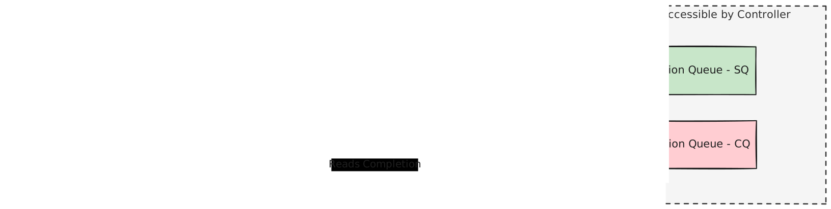
<p>On a high level NVMe works with queue pairs SQs(Submission Queues), CQs(Completion Queues), and doorbells. SQs/CQs live
in a memory the NVMe controller can access, usually system RAM. Then we just write commands in those queues and
ring the doorbells to inform the controller, it will DMA and access the SQ to read the commands and write to the
CQ.</p>
<p><img src="https://thegeeko.me/images/sq-cq-visualization.svg" alt="Simple SQ/CQ" /></p>
<p>There’s a special pair of queues called the admin queue which can be used to create I/O queues to transfer data,
and can also respond to an Identify command that gives us some information about the NVMe device.</p>
<p>For a proof of concept, we need a minimal test: submit an Identify command to the admin queue from
CPU, notify the controller from the GPU side, and place the returned data in VRAM. If that works, then the basic
NVMe -&gt; VRAM and GPU -&gt; BAR0 path is real.[^2]</p>
<p>[^2]: Later we will use I/O queues to write a file and read back using
<a href="https://github.com/enfiskutensykkel/ssd-gpu-dma">libnvm</a> by Jonas Markussen.</p>
<h1>VFIO, IOMMUFD, and IOAS</h1>
<p>Now for the Linux side of things.</p>
<p>VFIO lets user-space manage a physical PCIe device in a controlled way. For this post, the important part is
that it gives us access to PCIe BARs and lets us bind the device to an IOMMU-managed address space.</p>
<p>The latter part matters because the NVMe controller is a DMA-capable device. If user-space could just write any
physical addresses into the queue registers, the device would happily DMA there, which would be a complete
disaster.</p>
<p>Instead of handing the device raw physical addresses, we give it IOVAs, and the IOMMU translates those to the real backing memory. So from the controller’s point of view it is reading and writing some virtual I/O address space, and the kernel controls what that actually maps to.</p>
<p>IOMMUFD is the interface we use to program the IOMMU. It gives us the concept of an IOAS, an I/O address space.
We can create one, attach our VFIO-managed NVMe device to it, and then map either normal user memory or
DMA-BUF-backed memory into it.</p>
<p>This is what makes Path 1 possible. If we can map a VRAM-backed DMA-BUF into an IOAS, then the NVMe controller
can DMA directly into VRAM.</p>
<p>For Path 2 VFIO allows us to export the NVMe BAR0 as DMA-BUF[^3] which then we can map to the GPU VM.</p>
<p>[^3]: This is true in the tree I linked to earlier in[^1]</p>
<h1>What Is Missing</h1>
<p>At this point the shape of the problem is pretty clear.</p>
<p>For Path 1, we need IOMMUFD to accept a GPU allocation exported as a DMA-BUF and map it into the IOAS in a way a VFIO device could use.</p>
<p>For Path 2, we need the NVMe BAR to be exportable as a DMA-BUF, and we need a way to import that into
GPU-visible address space.</p>
<p>The <a href="https://lore.kernel.org/linux-iommu/0-v1-b5cab63049c0+191af-dmabuf_map_type_jgg@nvidia.com">DMA-BUF patches</a> is already
moving in the right direction, it replaces the old way of mapping the DMA-BUF <code>sg_tables</code> by a system of
negotiation, which allows both the exporter and the importer to agree on a mapping type that works for both.</p>
<p>The new mapping type which interest us here is PAL(Physical Address List), which allows us to share raw physical
address with the importer. IOMMUFD only accepts this type[^4], but the AMDGPU driver doesn’t support the PAL
mapping type.</p>
<p>[^4]: The patches thread expands on this.</p>
<h1>Path 1: NVMe -&gt; GPU</h1>
<p>We need to make the AMDGPU driver support PAL.</p>
<p>The first thing we need to do is pin the buffer. Once we expose physical address ranges, relocation becomes dangerous: if the driver moves the buffer after we hand those addresses to another device, the NVMe controller would keep DMAing to stale memory. Fortunately, AMDGPU already has DMA-BUF pinning.</p>
<pre><code class="language-c">static struct dma_buf_phys_list *
amdgpu_dma_buf_map_phys(struct dma_buf_attachment *attach)
{
	...
	r = amdgpu_dma_buf_pin(attach);
	if (r)
		return ERR_PTR(r);
</code></pre>
<p>Next we check that the buffer is actually backed by VRAM. If it lives in normal system memory, there is no need to go through this DMA-BUF path at all, because IOMMUFD can already map system memory directly.</p>
<pre><code class="language-c">	if (bo-&gt;tbo.resource-&gt;mem_type != TTM_PL_VRAM) {
		r = -EINVAL;
		goto error_free;
	}
</code></pre>
<p>Once the buffer is pinned and confirmed to live in VRAM, we can walk its backing store and build a PAL from the underlying physical ranges.</p>
<pre><code class="language-c">	r = amdgpu_vram_mgr_alloc_pal(adev, bo-&gt;tbo.resource, 0,
		bo-&gt;tbo.base.size, &amp;pal);
</code></pre>
<p>The function <code>amdgpu_vram_mgr_alloc_pal</code> is simple. It walks the VRAM resource block by block, counts how many ranges are needed, allocates the PAL, and then fills each entry with a physical address and a length. In this implementation, the physical address comes from the blocks offset into VRAM plus the GPU aperture base.</p>
<pre><code class="language-c">int amdgpu_vram_mgr_alloc_pal(struct amdgpu_device *adev,
			      struct ttm_resource *res, u64 offset, u64 length,
			      struct dma_buf_phys_list **pal)
{
	...
	while (cursor.remaining) {
		u64 i = (*pal)-&gt;length;

		(*pal)-&gt;phys[i].paddr = cursor.start + adev-&gt;gmc.aper_base;
		(*pal)-&gt;phys[i].len   = cursor.size;

		(*pal)-&gt;length += 1;
		amdgpu_res_next(&amp;cursor, cursor.size);
	}
	...
}

</code></pre>
<p>Then, we mark the buffer as uncached. The NVMe controller is now writing to this memory directly, outside the
GPU’s normal virtual-memory and cache-management path, so we need to avoid stale cached views of the data.</p>
<pre><code class="language-c">	bo-&gt;flags |= AMDGPU_GEM_CREATE_UNCACHED;
</code></pre>
<p>Now this function <code>amdgpu_dma_buf_map_phys</code> can get a PAL representing this buffer safely, we need to advertise
that we support PAL mapping. This function get invoked when negotiating. It should provide a list of
supported mappings we just add a struct that holds the <code>amdgpu_dma_buf_map_phys</code> and <code>amdgpu_dma_buf_unmap_phys</code>
functions.</p>
<pre><code class="language-c">static int amdgpu_dma_buf_match_mapping(struct dma_buf_match_args *args) {
	...
	if (peer2peer) {
		match[num_match++] = DMA_BUF_EMAPPING_PAL(&amp;amdgpu_dma_buf_pal_ops);
	}
	...
}
</code></pre>
<p>This should be enough to map VRAM-backed buffers to an IOAS.</p>
<h1>Path 2: GPU -&gt; NVMe BAR0</h1>
<p>Here, we don’t need any changes on the AMDGPU driver side[^5]. The heavy lifting is being done by the patches
that allows exporting NVMe BAR0 as a DMA-BUF, allowing us to map it directly to the GPU VM which makes the BAR0
visible to the GPU.</p>
<p>[^5]: At least in my setup.</p>
<p>Something worth mentioning here, is that if use the HIP API to import the DMA-BUF aka use
<code>hipMemImportFromShareableHandle</code> function it assumes the imported buffer is being exported by another AMD GPU.
Thankfully HSA EXT API does have <code>hsa_amd_interop_map_buffer</code> which its implementation much simpler and direct. A
small problem with <code>hsa_amd_interop_map_buffer</code> that internally it calls the IOCTL <code>AMDKFD_IOC_GET_DMABUF_INFO</code>,
which would error if the DMA-BUF is not exported by AMDGPU driver itself. I modified the function that handles
the ioctl to return a dummy info, I believe this should be fixed at the HSA level, but this would do for now.</p>
<pre><code class="language-c">int amdgpu_amdkfd_get_dmabuf_info(...)
{
	...
	if (dma_buf-&gt;ops != &amp;amdgpu_dmabuf_ops) {
		if (dmabuf_adev)
			*dmabuf_adev = adev;
		if (bo_size)
			*bo_size = dma_buf-&gt;size;
		if (metadata_size)
			*metadata_size = 0;
		if (flags)
			*flags = KFD_IOC_ALLOC_MEM_FLAGS_GTT |
				 KFD_IOC_ALLOC_MEM_FLAGS_UNCACHED |
				 KFD_IOC_ALLOC_MEM_FLAGS_WRITABLE;
		if (xcp_id)
			*xcp_id = -1;

		r = 0;
		goto out_put;
	}
	...
}
</code></pre>
<p>Now this should be enough for the most basic P2P communication.</p>
<h1>The User-Space Perspective</h1>
<p>Let’s make a simple prove of concept to assert that our plumbing here worked. A simple driver that rings the admin
queues doorbell from a shader(kernel), and should use the VRAM as the location of the command result. The rest
will be done from the CPU to make it simple for now.</p>
<p>The next part assumes that we have an NVMe device that is being managed by the VFIO driver. <code>lspci</code> command output
should look like this:</p>
<pre><code class="language-bash">lspci -k -nn -s 0000:04:00.0

04:00.0 Non-Volatile memory controller [0108]: Samsung Electronics Co Ltd NVMe SSD Controller SM981/PM981/PM983 [144d:a808]
	Subsystem: Samsung Electronics Co Ltd SSD 970 EVO/PRO [144d:a801]
	Kernel driver in use: vfio-pci # notice here
	Kernel modules: nvme
</code></pre>
<p>We can start by opening the IOMMUFD which will allow us to allocate an IOAS</p>
<pre><code class="language-c">s32 iommu_fd = open("/dev/iommu", O_RDWR);
struct iommu_ioas_alloc iommu_alloc_request = { ... };
ioctl(iommu_fd, IOMMU_IOAS_ALLOC, &amp;iommu_alloc_request);
</code></pre>
<p>Then we can open the VFIO char device and associate it with our IOAS</p>
<pre><code class="language-c">s32 vfio_fd = open("/dev/vfio/devices/vfio0", O_RDWR);
struct vfio_device_bind_iommufd vfio_bind_request = { ... };
ioctl(vfio_fd, VFIO_DEVICE_BIND_IOMMUFD, &amp;vfio_bind_request);

struct vfio_device_attach_iommufd_pt vfio_attach_request = { ... };
ioctl(vfio_fd, VFIO_DEVICE_ATTACH_IOMMUFD_PT, &amp;vfio_attach_request);
</code></pre>
<p>By now we have control over our nvme device, we can query info about PCIe regions, etc. We care about exporting NVMe BAR0 we can make use of the features added by patches I mentioned earlier, as we can see here:</p>
<pre><code class="language-c">  pci_feature_req-&gt;argsz = pci_feature_req_size;
  pci_feature_req-&gt;flags =
    VFIO_DEVICE_FEATURE_GET | VFIO_DEVICE_FEATURE_DMA_BUF;

  pci_feature_req_dma-&gt;region_index         = 0;
  pci_feature_req_dma-&gt;open_flags           = O_RDWR | O_CLOEXEC;
  pci_feature_req_dma-&gt;nr_ranges            = 1;
  pci_feature_req_dma-&gt;dma_ranges[0].offset = 0;
  pci_feature_req_dma-&gt;dma_ranges[0].length = vfio_bar0_region_info.size;

  s32 bar0_dmabuf_fd =
    ioctl(vfio_device_file_descriptor, VFIO_DEVICE_FEATURE, pci_feature_req);
</code></pre>
<p>At this point <code>bar0_dmabuf_fd</code> refers to the NVMe BAR0 we can map that using the function
<code>hsa_amd_interop_map_buffer</code> I mentioned earlier.</p>
<p>Now let’s allocate some buffer on the VRAM and export them, thankfully the HIP API makes this simple.</p>
<pre><code class="language-c">hipMemAllocationProp props = { ... };
hipMemGenericAllocationHandle_t alloc_handle;
hipMemCreate(&amp;alloc_handle, dma_buffer_size, &amp;props, 0);

void *gpu_va;
hipMemAddressReserve(&amp;gpu_va, dma_buffer_size, 4096, NULL, 0);
hipMemMap(gpu_va, dma_buffer_size, 0, alloc_handle, 0);

hipMemAccessDesc access = { ... };
hipMemSetAccess(gpu_va, dma_buffer_size, &amp;access, 1);

int result_dmabuf_fd;
hipMemExportToShareableHandle(&amp;result_dmabuf_fd, alloc_handle,
                              hipMemHandleTypePosixFileDescriptor, 0);
</code></pre>
<p>At this point <code>result_dmabuf_fd</code> refers to the buffer we allocated for the NVMe to store the result of Identify
command into, and we can map it into our IOAS using <code>IOMMU_IOAS_MAP_FILE</code> IOCTL.</p>
<p>Here we should map the NVMe BAR0 to the CPU side too and set up the NVMe controller and admin queues I won’t
include those here but you can see the full source code of this proof of concept
<a href="https://codeberg.org/a_hadi/nvme_gpu_p2p_amdgpu/src/branch/master/standalone-basic">here</a>.</p>
<p>After we set up admin queues and we can write an Identify command that uses the VRAM for the result as follows:</p>
<pre><code class="language-c">  nvme_sqe_t identify_cmd = {
    .opc   = 0x06, // Identify command opcode
    .cid   = 1,
    .prp1  = result_iova, // we got this from the IOMMU_IOAS_MAP_FILE ioctl
    .cdw10 = 1,
  };

  admin_submission_queue[0] = identify_cmd;
</code></pre>
<p>Now everything is ready to run the GPU shaders and ring the doorbell, the shader is very simple just writes 1
to the doorbell register</p>
<pre><code class="language-c">__global__ void ring_doorbell_kernel(volatile u32* queue_doorbell) {
  *queue_doorbell = 1;
}
</code></pre>
<p>From the CPU side, we just poll the admin CQ and once it’s done, we can copy back the data from the GPU VRAM
and we see:</p>
<pre><code class="language-bash">NVMe Identfication Info:
  Vendor ID: 0x144d
  Subsystem Vendor ID: 0x144d
  Serial Number: S5H7NS0N845653J
  Model Number: Samsung SSD 970 EVO 500GB
  Firmware Revision: 2B2QEXE7
</code></pre>
<p>It works! Now let’s do data transfers and enqueue and do the polling from the GPU side.</p>
<h1>GPU Driven I/O</h1>
<p>At this point, I did not want to write a user-space NVMe driver from scratch just to validate the kernel plumbing.
I already had a much better starting point <a href="https://github.com/enfiskutensykkel/ssd-gpu-dma">libnvm</a>, Jonas
Markussen’s user-space NVMe library, which was built around the same general idea of low-level queue control and
GPU-driven I/O.</p>
<p>I won’t talk much about the porting process since we already talked about the interesting parts if you’re curious
take a look at the port and some examples <a href="https://codeberg.org/a_hadi/nvme_gpu_p2p_amdgpu">here</a>.</p>
<p>Now with the port in place, let’s take a look at an example shader that writes or reads a file from the NVMe
device. Again there’s a lot of boilerplate code I won’t show here but can see it and run it for yourself
<a href="https://codeberg.org/a_hadi/nvme_gpu_p2p_amdgpu/src/branch/master/examples">here</a>.</p>
<p>In this shader, each GPU thread owns one queue pair, takes responsibility for one slice of the transfer, submits
NVMe read or write commands through its own submission queue, and then drains completions from the respective
completion queue.</p>
<p>The first thing the kernel does is assign one queue pair per GPU thread. That keeps the control flow simple.</p>
<pre><code class="language-c">uint32_t tid = blockIdx.x * blockDim.x + threadIdx.x;
if (tid &gt;= n_queues) return;

nvm_queue_t* sq = sqs + tid;
nvm_queue_t* cq = cqs + tid;
</code></pre>
<p>Now we can construct our read or write commands, libnvm handles that nicely for us the thing to notice here is
we are using address directly which was made possible by the plumbing work we did earlier. The NVMe can DMA
directly into <code>sq-&gt;vaddr</code> which holds the VRAM memory for the SQ, and <code>sq-&gt;ioaddr</code> is the IOVA of that same
memory.</p>
<pre><code class="language-c">nvm_cmd_header(cmd, cid, write ? NVM_IO_WRITE : NVM_IO_READ, ns_id);

size_t global_page = thread_base_page + page_offset;
size_t start_block = NVM_PAGE_TO_BLOCK(page_size, block_size, global_page);
size_t n_blocks    = NVM_PAGE_TO_BLOCK(page_size, block_size, xfer_pages);

nvm_cmd_rw_blks(cmd, start_block, n_blocks);
nvm_cmd_data(
  cmd, page_size, xfer_pages,
  NVM_PTR_OFFSET(sq-&gt;vaddr, page_size, prp_slot),
  NVM_ADDR_OFFSET(sq-&gt;ioaddr, page_size, prp_slot),
  data_ioaddrs + global_page
);
</code></pre>
<p>Now the thread can submit the work and drain the CQ, this is easy because libnvm is built around polling rather
than interrupts. The next code will show the 2 paths we paved earlier in action. <code>nvm_sq_submit</code> will ring the
NVMe doorbell(GPU -&gt; NVMe), and the NVMe will write back to the CQ which lives in GPU VRAM.</p>
<pre><code class="language-c">nvm_sq_submit(sq);

while (cmds_completed &lt; cmds_submitted) {
  nvm_cpl_t* cpl = nvm_cq_dequeue(cq);
  if (cpl == NULL)
    continue;

  if (!NVM_ERR_OK(cpl)) {
    printf("NVMe completion error ...\n");
    return;
  }

  nvm_sq_update(sq);
  nvm_cq_update(cq);
  cmds_completed++;
}
</code></pre>
<p>Running this, and it doesn’t work it gets stuck in CQ polling</p>
<h1>Cache Coherency</h1>
<p>The first path is the tricky one, so let’s start with the second path GPU -&gt; NVMe. Here we have to just make sure
we skip L2 and MALL cache. From <a href="https://thegeeko.me/blog/amd-gpu-debugging/">the debugger experiments</a>, we know
if we set the mapping type(MTYPE) to uncached(UC) the RDNA3 GPUs skip it. So we make sure our SQs are allocated
with uncached flag.</p>
<pre><code class="language-c">hsa_err   = hsa_amd_memory_pool_allocate(
  vram_pool, size, HSA_AMD_MEMORY_POOL_UNCACHED_FLAG, &amp;ptr
);
</code></pre>
<p>This is probably overkill and we can do a <code>__threadfence_system()</code> before ringing the doorbell, but allocating
both SQs and CQs the same way makes the code simpler so I’m ignoring this for now. It’s also worth mentioning
when we export the buffer as PAL we do add uncached flag but it wasn’t reliable in my experience[^6].</p>
<p>[^6]: We can check the actual MTYPE value at the end by decoding the page table using UMR.</p>
<p>Now for the other side NVMe -&gt; VRAM, when the NVMe controller is done it writes back to CQs and it DMA directly
using the physical address. We need to make sure that there’s no inbound PCIe traffic buffering, and all our GPU
reads skip all possible caches.</p>
<p>For the later part the combination of <code>MTYPE=UC</code> and <code>glc slc dlc</code> modifers on the load instruction should suffice
as you can see here:</p>
<pre><code class="language-c">__host__ __device__ static inline nvm_cpl_t*
nvm_cq_poll(const nvm_queue_t* cq) {
  ...
#ifdef __HIP_DEVICE_COMPILE__
  asm volatile(
    "global_load_u16 %0, %1, off glc slc dlc\n\t"
    "s_waitcnt vmcnt(0)"
    : "=v"(raw)
    : "v"(status_addr)
    : "memory"
  );

  ...
}
</code></pre>
<p>Now by just running this it still reads stale data, not the NVMe CQ entries.</p>
<p><strong>This was tough to debug, and I learned from it, but take the next part with a grain of salt, it may contain wrong information if you saw any please contact me, I’ll fix, and I want to know ;).</strong></p>
<p>So I had no idea how to approach this, but I noticed when I open anything that uses the AMD GPU for
rendering[^7] it works but it was a bit random it always worked but not at set intervals. I minimized the
surface and switched to raw PM4 packets submissions and tracked down to a couple of things.</p>
<p>[^7]: I use an Nvidia GPU for display so the AMD GPU stays idle unless I force some workload to use it.</p>
<p>I found something called HDP(Host Data Path) cache, but in the <a href="https://codeberg.org/a_hadi/linux_p2p_dma_amdgpu/src/commit/8ab25043a85358758c771259ab298ee3d2ddd4af/drivers/gpu/drm/amd/amdgpu/amdgpu_discovery.c#L2965">amdgpu_discovery.c</a> file there’s no mention for GFX11(RX 7900XTX) and HDP together, but I looked into the <code>nbio_v7_7.c</code> version, and found this:</p>
<pre><code class="language-c">static u32 nbio_v7_7_get_hdp_flush_req_offset(struct amdgpu_device *adev)
{
	return SOC15_REG_OFFSET(NBIO, 0, regBIF_BX_PF0_GPU_HDP_FLUSH_REQ);
}
</code></pre>
<p>Using UMR to poke around the <code>BIF_BX_PF&lt;X&gt;_GPU_HDP_FLUSH_REQ</code> didn’t do anything, and the shader was stuck
polling still.</p>
<p>Next up I tracked a couple of paths and found <code>GCR_GENERAL_CNTL</code>, <code>GCVM_L2_CNTL2</code> and
<code>GCVM_INVALIDATE_ENG&lt;X&gt;_REQ</code> registers, playing with the first two triggered a GPU reset, but the last one did
the trick and made the CQs entries visible to the GPU.</p>
<p>There’s multiple <code>GCVM_INVALIDATE_ENG&lt;X&gt;_REQ</code> registers 0-17, and the structure of the register is:</p>
<pre><code class="language-c">typedef union {
	struct {
		uint32_t per_vmid_invalidate_req : 16;
		uint32_t flush_type : 3;
		uint32_t invalidate_l2_ptes : 1;
		uint32_t invalidate_l2_pde0 : 1;
		uint32_t invalidate_l2_pde1 : 1;
		uint32_t invalidate_l2_pde2 : 1;
		uint32_t invalidate_l1_ptes : 1;
		uint32_t clear_protection_fault_status_addr : 1;
		uint32_t log_request : 1;
		uint32_t invalidate_4k_pages_only : 1;
	};
	uint32_t raw;
} reg_gcvm_invalidate_eng17_req_t;
</code></pre>
<p>Turned out that only <code>eng17</code> register, <code>flush_type = 2</code>, and a nonzero <code>per_vmid_invalidate_req</code> work. The
<code>per_vmid_invalidate_req</code> is a mask with each bit corresponding to a VMID[^8], and it feels like an early return
check if it has no VMID bit enabled. The <code>flush_type</code> is the interesting part here on <code>flush_type = 2</code> from
<a href="https://lists.freedesktop.org/archives/amd-gfx/2025-February/120529.html">this patch</a> we can know it stands for
heavy-weight flush.</p>
<p>[^8]: I explained the VMIDs before, read about it <a href="https://thegeeko.me/blog/amd-gpu-debugging/#amdgpu-debugfs">here</a>.</p>
<p>And from <a href="https://codeberg.org/a_hadi/linux_p2p_dma_amdgpu/src/commit/8ab25043a85358758c771259ab298ee3d2ddd4af/drivers/gpu/drm/amd/amdgpu/amdgpu_gmc.c#L577">here</a> we know ENG17 is allocated for GART flushes. The kernel documentation
define GART as:</p>
<blockquote>
<p>Graphics Address Remapping Table. This is the name we use for the GPUVM page table used by the GPU kernel
driver. It remaps system resources (memory or MMIO space) into the GPU’s address space so the GPU can access
them. The name GART harkens back to the days of AGP when the platform provided an MMU that the GPU could use to
get a contiguous view of scattered pages for DMA. The MMU has since moved on to the GPU, but the name stuck.</p>
</blockquote>
<p>This whole thing didn’t make sense to me. <code>GCVM_INVALIDATE_ENG&lt;X&gt;_REQ</code> seems to be used to flush TLB, and this
shouldn’t affect the data visibility if we already have the correct address mapped. I verified using UMR page
decoding before and after the flush it was the exact same, and the page tables are per VMID, and toggling any of
the VMID bits works not the one specific to our PSID.</p>
<p>What I think is going here is this is an unintended side effect of a heavy-weight flush which is unlikely, or
this GART have an internal buffering or cache that is not exposed to the KMD. It’s also worth mentioning that
<code>GCVM_INVALIDATE_ENG&lt;X&gt;_REQ</code> are a <code>gfxhub</code> registers and there’s another <code>MMVM_INVALIDATE_ENG&lt;X&gt;_REQ</code> group of
registers which are a <code>mmhub</code> registers but those don’t have the same effect as the <code>gfxhub</code> ones, so maybe
it’s something inside the <code>gfxhub</code>. We can’t truly know without knowing how those parts of the hardware work.</p>
<p>I made a simple program that uses debugfs interface to keep poking the register and invalidate the cache it
assumes GFX11 tho. If you want to run the code on another GPU use UMR to poke it manually.</p>
<p>With those things in place the examples work correctly, writing a file and then reading it back result in the
same file.</p>
<h1>You can run them yourself</h1>
<ul>
<li><a href="https://codeberg.org/a_hadi/linux_p2p_dma_amdgpu">the linux kernel</a></li>
<li><a href="https://codeberg.org/a_hadi/nvme_gpu_p2p_amdgpu">libnvm and the examples</a></li>
</ul>
<hr />
<p><strong>Hi again, if you liked what you read I’m graduating at the end of this month. Consider hiring me or referring me:</strong></p>
<ul>
<li><a href="https://linkedin.com/in/thegeeko">Linkedin</a></li>
<li><a href="/resume.pdf">Resume</a></li>
<li>Email me at: <a href="mailto:abdelhadims@icloud.com">abdelhadims@icloud.com</a></li>
</ul>
]]></content>
        <published>2026-03-16T00:00:00.000Z</published>
    </entry>
    <entry>
        <title type="html"><![CDATA[AMD GPU Debugger]]></title>
        <id>https://thegeeko.me/blog/amd-gpu-debugging</id>
        <link href="https://thegeeko.me/blog/amd-gpu-debugging"/>
        <updated>2025-12-06T00:00:00.000Z</updated>
        <content type="html"><![CDATA[<p>I’ve always wondered why we don’t have a GPU debugger similar to the one used for CPUs. A tool that allows pausing execution and examining the current state. This capability feels essential, especially since the GPU’s concurrent execution model is much harder to reason about. After searching for solutions, I came across rocgdb, a debugger for AMD’s ROCm environment. Unfortunately, its scope is limited to that environment. Still, this shows it’s technically possible. I then found a helpful <a href="https://martty.github.io/posts/radbg_part_1/">series of blog posts</a> by <a href="https://martty.github.io/about/">Marcell Kiss</a>, detailing how he achieved this, which inspired me to try to recreate the process myself.</p>
<h1>Let’s Try To Talk To The GPU Directly</h1>
<p>The best place to start learning about this is <a href="https://docs.mesa3d.org/drivers/radv.html">RADV</a>. By tracing what it does, we can find how to do it. Our goal here is to run the most basic shader <code>nop 0</code> without using Vulkan, aka RADV in our case.</p>
<p>First of all, we need to open the DRM file to establish a connection with the KMD, using a simple open(“/dev/dri/cardX”), then we find that it’s calling <code>amdgpu_device_initialize</code>, which is a function defined in <code>libdrm</code>, which is a library that acts as middleware between user mode drivers(UMD) like <code>RADV</code> and and kernel mode drivers(KMD) like amdgpu driver, and then when we try to do some actual work we have to create a context which can be achieved by calling <code>amdgpu_cs_ctx_create</code> from <code>libdrm</code> again, next up we need to allocate 2 buffers one of them for our code and the other for writing our commands into, we do this by calling a couple of functions, here’s how I do it:</p>
<pre><code class="language-c">void bo_alloc(amdgpu_t* dev, size_t size, u32 domain, bool uncached, amdgpubo_t* bo) {
 s32    ret         = -1;
 u32    alignment   = 0;
 u32    flags       = 0;
 size_t actual_size = 0;

 amdgpu_bo_handle bo_handle = NULL;
 amdgpu_va_handle va_handle = NULL;
 u64              va_addr   = 0;
 void*            host_addr = NULL;
</code></pre>
<p>Here we’re choosing the domain and assigning flags based on the params, some buffers we will need uncached, as we will see:</p>
<pre><code class="language-c"> if (
   domain != AMDGPU_GEM_DOMAIN_GWS &amp;&amp; domain != AMDGPU_GEM_DOMAIN_GDS &amp;&amp;
   domain != AMDGPU_GEM_DOMAIN_OA) {
  actual_size = (size + 4096 - 1) &amp; 0xFFFFFFFFFFFFF000ULL;
  alignment   = 4096;
  flags       = AMDGPU_GEM_CREATE_CPU_ACCESS_REQUIRED | AMDGPU_GEM_CREATE_VRAM_CLEARED |
          AMDGPU_GEM_CREATE_VM_ALWAYS_VALID;
  flags |=
    uncached ? (domain == AMDGPU_GEM_DOMAIN_GTT) * AMDGPU_GEM_CREATE_CPU_GTT_USWC : 0;
 } else {
  actual_size = size;
  alignment   = 1;
  flags       = AMDGPU_GEM_CREATE_NO_CPU_ACCESS;
 }

 struct amdgpu_bo_alloc_request req = {
  .alloc_size     = actual_size,
  .phys_alignment = alignment,
  .preferred_heap = domain,
  .flags          = flags,
 };

 // memory aquired!!
 ret = amdgpu_bo_alloc(dev-&gt;dev_handle, &amp;req, &amp;bo_handle);
 HDB_ASSERT(!ret, "can't allocate bo");
</code></pre>
<p>Now we have the memory, we need to map it. I opt to map anything that can be CPU-mapped for ease of use. We have to map the memory to both the GPU and the CPU virtual space. The KMD creates the page table when we open the DRM file, as shown <a href="https://elixir.bootlin.com/linux/v6.18/source/drivers/gpu/drm/amd/amdgpu/amdgpu_kms.c#L1425">here</a>.</p>
<p>So map it to the GPU VM and, if possible, to the CPU VM as well. Here, at this point, there’s a libdrm function that does all of this setup for us and maps the memory, but I found that even when specifying <code>AMDGPU_VM_MTYPE_UC</code>, it doesn’t always tag the page as uncached, not quite sure if it’s a
bug in my code or something in <code>libdrm</code> anyways, the function is <code>amdgpu_bo_va_op</code>, I opted to do it manually here and issue the IOCTL call myself:</p>
<pre><code class="language-c"> u32 kms_handle = 0;
 amdgpu_bo_export(bo_handle, amdgpu_bo_handle_type_kms, &amp;kms_handle);

 ret = amdgpu_va_range_alloc(
   dev-&gt;dev_handle,
   amdgpu_gpu_va_range_general,
   actual_size,
   4096,
   0,
   &amp;va_addr,
   &amp;va_handle,
   0);
 HDB_ASSERT(!ret, "can't allocate VA");

 u64 map_flags =
   AMDGPU_VM_PAGE_EXECUTABLE | AMDGPU_VM_PAGE_READABLE | AMDGPU_VM_PAGE_WRITEABLE;
 map_flags |= uncached ? AMDGPU_VM_MTYPE_UC | AMDGPU_VM_PAGE_NOALLOC : 0;

 struct drm_amdgpu_gem_va va = {
  .handle       = kms_handle,
  .operation    = AMDGPU_VA_OP_MAP,
  .flags        = map_flags,
  .va_address   = va_addr,
  .offset_in_bo = 0,
  .map_size     = actual_size,

 };

 ret = drm_ioctl_write_read(dev-&gt;drm_fd, DRM_AMDGPU_GEM_VA, &amp;va, sizeof(va));
 HDB_ASSERT(!ret, "can't map bo in GPU space");
 // ret = amdgpu_bo_va_op(bo_handle, 0, actual_size, va_addr, map_flags,
 // AMDGPU_VA_OP_MAP);

 if (flags &amp; AMDGPU_GEM_CREATE_CPU_ACCESS_REQUIRED) {
  ret = amdgpu_bo_cpu_map(bo_handle, &amp;host_addr);
  HDB_ASSERT(!ret, "can't map bo in CPU space");

  // AMDGPU_GEM_CREATE_VRAM_CLEARED doesn't really memset the memory to 0 anyways for
  // debug I'll just do it manually for now
  memset(host_addr, 0x0, actual_size);
 }

 *bo = (amdgpubo_t){
  .bo_handle = bo_handle,
  .va_handle = va_handle,
  .va_addr   = va_addr,
  .size      = actual_size,
  .host_addr = host_addr,
 };
}
</code></pre>
<p>Now we have the context and 2 buffers. Next, fill those buffers and send our commands to the KMD, which will then forward them to the Command Processor (CP) in the GPU for processing.</p>
<p>Let’s compile our code. We can use clang assembler for that, like this:</p>
<pre><code class="language-c"># https://gitlab.freedesktop.org/martty/radbg-poc/-/blob/master/ll-as.sh
clang -c -x assembler -target amdgcn-amd-amdhsa -mcpu=gfx1100 -o asm.o "$1"
objdump -h asm.o | grep .text | awk '{print "dd if='asm.o' of='asmc.bin' bs=1 count=$[0x" $3 "] skip=$[0x" $6 "] status=none"}' | bash
#rm asm.o
</code></pre>
<p>The bash script compiles the code, and then we’re only interested in the actual machine code, so we use objdump to figure out the offset and the size of the section and copy it to a new file called asmc.bin, then we can just load the file and write its bytes to the CPU-mapped address of the code buffer.</p>
<p>Next up, filling in the commands. This was extremely confusing for me because it’s not well documented.
It was mostly learning how <code>RADV</code> does things and trying to do similar things. Also, shout-out to the folks on the Graphics Programming Discord server for helping me, especially Picoduck. The commands are encoded in a special format called <code>PM4 Packets</code>, which has multiple types. We only care about <code>Type 3</code>: each packet has an opcode and the number of bytes it contains.</p>
<p>The first thing we need to do is program the GPU registers, then dispatch the shader. Some of those registers are <code>rsrc[1-3]</code>; those registers are responsible for a number of configurations, pgm_[lo/hi], which hold the pointer to the code buffer and <code>num_thread_[x/y/z]</code>; those are responsible for the number of threads inside a work group. All of those are set using the <code>set shader register</code> packets, and here is how to encode them:</p>
<p>{% mark %} It’s worth mentioning that we can set multiple registers in 1 packet if they’re consecutive.{% /mark %}</p>
<pre><code class="language-c">void pkt3_set_sh_reg(pkt3_packets_t* packets, u32 reg, u32 value) {
 HDB_ASSERT(
   reg &gt;= SI_SH_REG_OFFSET &amp;&amp; reg &lt; SI_SH_REG_END,
   "can't set register outside sh registers span");

 // packet header
 da_append(packets, PKT3(PKT3_SET_SH_REG, 1, 0));
 // offset of the register
 da_append(packets, (reg - SI_SH_REG_OFFSET) / 4);
 da_append(packets, value);
}
</code></pre>
<p>Then we append the dispatch command:</p>
<pre><code class="language-c">// we're going for 1 thread since we want the simplest case here.

da_append(&amp;pkt3_packets, PKT3(PKT3_DISPATCH_DIRECT, 3, 0) | PKT3_SHADER_TYPE_S(1));
da_append(&amp;pkt3_packets, 1u);
da_append(&amp;pkt3_packets, dispatch_initiator);
</code></pre>
<p>Now we want to write those commands into our buffer and send them to the KMD:</p>
<pre><code class="language-c">void dev_submit(
  amdgpu_t*         dev,
  pkt3_packets_t*   packets,
  amdgpu_bo_handle* buffers,
  u32               buffers_count,
  amdgpu_submit_t*  submit
) {
 s32        ret = -1;
 amdgpubo_t ib  = { 0 };

 bo_alloc(dev, pkt3_size(packets), AMDGPU_GEM_DOMAIN_GTT, false, &amp;ib);
 bo_upload(&amp;ib, packets-&gt;data, pkt3_size(packets));

 amdgpu_bo_handle* bo_handles = // +1 for the indirect buffer
   (amdgpu_bo_handle*)malloc(sizeof(amdgpu_bo_handle) * (buffers_count + 1));

 bo_handles[0] = ib.bo_handle;
 for_range(i, 0, buffers_count) {
  bo_handles[i + 1] = buffers[i];
 }

 amdgpu_bo_list_handle bo_list = NULL;
 ret =
   amdgpu_bo_list_create(dev-&gt;dev_handle, buffers_count + 1, bo_handles, NULL, &amp;bo_list);
 HDB_ASSERT(!ret, "can't create a bo list");
 free(bo_handles);

 struct amdgpu_cs_ib_info ib_info = {
  .flags         = 0,
  .ib_mc_address = ib.va_addr,
  .size          = packets-&gt;count,
 };

 struct amdgpu_cs_request req = {
  .flags                  = 0,
  .ip_type                = AMDGPU_HW_IP_COMPUTE,
  .ip_instance            = 0,
  .ring                   = 0,
  .resources              = bo_list,
  .number_of_dependencies = 0,
  .dependencies           = NULL,
  .number_of_ibs          = 1,
  .ibs                    = &amp;ib_info,
  .seq_no                 = 0,
  .fence_info             = { 0 },
 };

 ret = amdgpu_cs_submit(dev-&gt;ctx_handle, 0, &amp;req, 1);
 HDB_ASSERT(!ret, "can't submit indirect buffer request");

 *submit = (amdgpu_submit_t){
    .ib = ib,
    .bo_list = bo_list,
    .fence = {
      .context = dev-&gt;ctx_handle,
      .ip_type = AMDGPU_HW_IP_COMPUTE,
      .ip_instance = 0,
      .ring = 0,
      .fence = req.seq_no,
    },
  };
}
</code></pre>
<p>{% mark %}
Here is a good point to make a more complex shader that outputs something. For example, writing 1 to a buffer.
{% /mark %}</p>
<p>No GPU hangs ?! nothing happened ?! cool, cool, now we have a shader that runs on the GPU, what’s next? Let’s try to hang the GPU by pausing the execution, aka make the GPU trap.</p>
<h1>TBA/TMA</h1>
<p>The RDNA3’s ISA manual does mention 2 registers, <code>TBA, TMA</code>; here’s how they describe them respectively:</p>
<blockquote>
<p>Holds the pointer to the current trap handler program address. Per-VMID register. Bit [63] indicates if the trap
handler is present (1) or not (0) and is not considered part of the address
(bit[62] is replicated into address bit[63]).  Accessed via S_SENDMSG_RTN.</p>
</blockquote>
<blockquote>
<p>Temporary register for shader operations. For example, it can hold a pointer to memory used by the trap handler.</p>
</blockquote>
<p>{%mark%}
You can configure the GPU to enter the trap handler when encountering certain exceptions listed in the RDNA3 ISA manual.
{%/mark%}</p>
<p>We know from <a href="https://martty.github.io/about/">Marcell Kiss’s</a> blog posts that we need to compile a trap handler, which is a normal shader the GPU switches to when encountering a <code>s_trap</code>. The TBA register has a special bit that indicates whether the trap handler is enabled.</p>
<p>Since these are privileged registers, we cannot write to them from user space. To bridge this gap for debugging, we can utilize the debugfs interface. Luckily, we have <a href="https://umr.readthedocs.io/en/main/intro.html">UMR</a>, which uses that debugfs interface, and it’s open source; we copy AMD’s homework here which is great.</p>
<h1>AMDGPU Debugfs</h1>
<p>The amdgpu KMD has a couple of files in debugfs under <code>/sys/kernel/debug/dri/{PCI address}</code>; one of them is <code>regs2</code>, which is an interface to a <a href="https://elixir.bootlin.com/linux/v6.18/source/drivers/gpu/drm/amd/amdgpu/amdgpu_debugfs.c#L369"><code>amdgpu_debugfs_regs2_write</code></a> in the kernel that writes to the registers. It works by simply opening the file, seeking the register’s offset, and then writing; it also performs some synchronisation and writes the value correctly. We need to provide more parameters about the register before writing to the file, tho and do that by using an ioctl call. Here are the ioctl arguments:</p>
<pre><code class="language-c">typedef struct amdgpu_debugfs_regs2_iocdata_v2 {
 __u32 use_srbm, use_grbm, pg_lock;
 struct {
  __u32 se, sh, instance;
 } grbm;
 struct {
  __u32 me, pipe, queue, vmid;
 } srbm;
 __u32 xcc_id;
} regs2_ioc_data_t;
</code></pre>
<p>The 2 structs are because there are 2 types of registers, GRBM and SRBM, each of which is banked by different constructs; you can learn more about some of them here in <a href="https://docs.kernel.org/gpu/amdgpu/driver-core.html#gfx-compute-and-sdma-overall-behaviour">the Linux kernel documentation</a>.</p>
<p>Turns out our registers here are SBRM registers and banked by VMIDs, meaning each VMID has its own TBA and TMA registers. Cool, now we need to figure out the VMID of our process. As far as I understand, VMIDs are a way for the GPU to identify a specific process context, including the page table base address, so the address translation unit can translate a virtual memory address. The context is created when we open the DRM file. They get assigned dynamically at dispatch time, which is a problem for us; we want to write to those registers before dispatch.</p>
<p>We can obtain the VMID of the dispatched process by querying the <code>HW_ID2</code> register with s_getreg_b32. I do a hack here, by enabling the trap handler in every VMID, and there are 16 of them, the first being special, and used by the KMD and the last 8 allocated to the amdkfd driver. We loop over the remaining VMIDs and write to those registers. This can cause issues to other processes using other VMIDs by enabling trap handlers in them and writing the virtual address of our trap handler, which is only valid within our virtual memory address space. It’s relatively safe tho since most other processes won’t cause a trap[^1].</p>
<p>[^1]: Other processes need to have a s_trap instruction or have trap on exception flags set, which is not true for most normal GPU processes.</p>
<p>Now we can write to TMA and TBA, here’s the code:</p>
<pre><code class="language-c">void dev_op_reg32(
  amdgpu_t* dev, gc_11_reg_t reg, regs2_ioc_data_t ioc_data, reg_32_op_t op, u32* value) {
 s32 ret = 0;

 reg_info_t reg_info     = gc_11_regs_infos[reg];
 uint64_t   reg_offset   = gc_11_regs_offsets[reg];
 uint64_t   base_offset  = dev-&gt;gc_regs_base_addr[reg_info.soc_index];
 uint64_t   total_offset = (reg_offset + base_offset);

 // seems like we're multiplying by 4 here because the registers database in UMRs
 // source has them in indexes rather than bytes.
 total_offset *= (reg_info.type == REG_MMIO) ? 4 : 1;

 ret = hdb_ioctl(dev-&gt;regs2_fd, AMDGPU_DEBUGFS_REGS2_IOC_SET_STATE_V2, &amp;ioc_data);
 HDB_ASSERT(!ret, "Failed to set registers state");

 size_t size = lseek(dev-&gt;regs2_fd, total_offset, SEEK_SET);
 HDB_ASSERT(size == total_offset, "Failed to seek register address");

 switch (op) {
 case REG_OP_READ : size = read(dev-&gt;regs2_fd, value, 4); break;
 case REG_OP_WRITE: size = write(dev-&gt;regs2_fd, value, 4); break;
 default          : HDB_ASSERT(false, "unsupported op");
 }

 HDB_ASSERT(size == 4, "Failed to write/read the values to/from the register");
}
</code></pre>
<p>And here’s how we write to <code>TMA</code> and <code>TBA</code>:
{%mark%}
If you noticed, I’m using bitfields. I use them because working with them is much easier than macros, and while the byte order is not guaranteed by the C spec, it’s guaranteed by System V ABI, which Linux adheres to.
{%/mark%}</p>
<pre><code class="language-c">void dev_setup_trap_handler(amdgpu_t* dev, u64 tba, u64 tma) {
 reg_sq_shader_tma_lo_t tma_lo = { .raw = (u32)(tma) };
 reg_sq_shader_tma_hi_t tma_hi = { .raw = (u32)(tma &gt;&gt; 32) };

 reg_sq_shader_tba_lo_t tba_lo = { .raw = (u32)(tba &gt;&gt; 8) };
 reg_sq_shader_tba_hi_t tba_hi = { .raw = (u32)(tba &gt;&gt; 40) };

 tba_hi.trap_en = 1;

 regs2_ioc_data_t ioc_data = {
  .use_srbm = 1,
  .xcc_id   = -1,
 };

 // NOTE(hadi):
 // vmid's get assigned when code starts executing before hand we don't know which vmid
 // will get assigned to our process so we just set all of them
 for_range(i, 1, 9) {
  ioc_data.srbm.vmid = i;
  dev_op_reg32(dev, REG_SQ_SHADER_TBA_LO, ioc_data, REG_OP_WRITE, &amp;tba_lo.raw);
  dev_op_reg32(dev, REG_SQ_SHADER_TBA_HI, ioc_data, REG_OP_WRITE, &amp;tba_hi.raw);

  dev_op_reg32(dev, REG_SQ_SHADER_TMA_LO, ioc_data, REG_OP_WRITE, &amp;tma_lo.raw);
  dev_op_reg32(dev, REG_SQ_SHADER_TMA_HI, ioc_data, REG_OP_WRITE, &amp;tma_hi.raw);
 }
}
</code></pre>
<p>Anyway, now that we can write to those registers, if we enable the trap handler correctly, the GPU should hang when we launch our shader if we added <code>s_trap</code> instruction to it, or we enabled the <code>TRAP_ON_START</code> bit in rsrc3[^2] register.</p>
<p>[^2]: Available since RDNA3, if I’m not mistaken.</p>
<p>Now, let’s try to write a trap handler.</p>
<h1>The Trap Handler</h1>
<p>{%mark%}
If you wrote a different shader that outputs to a buffer, u can try writing to that shader from the trap handler, which is nice to make sure it’s actually being run.
{%/mark%}</p>
<p>We need 2 things: our trap handler and some scratch memory to use when needed, which we will store the address of in the TMA register.</p>
<p>The trap handler is just a normal program running in privileged state, meaning we have access to special registers like TTMP[0-15]. When we enter a trap handler, we need to first ensure that the state of the GPU registers is saved, just as the kernel does for CPU processes when context-switching, by saving a copy of the stable registers and the program counter, etc. The problem, tho, is that we don’t have a stable ABI for GPUs, or at least not one I’m aware of, and compilers use all the registers they can, so we need to save everything.</p>
<p>AMD GPUs’ Command Processors (CPs) have context-switching functionality, and the amdkfd driver does implement some <a href="https://elixir.bootlin.com/linux/v6.18/source/drivers/gpu/drm/amd/amdkfd/cwsr_trap_handler_gfx10.asm">context-switching shaders</a>. The problem is they’re not documented, and we have to figure them out from the amdkfd driver source and from other parts of the driver stack that interact with it, which is a pain in the ass. I kinda did a workaround here since I didn’t find luck understanding how it works, and some other reasons I’ll discuss later in the post.</p>
<p>The workaround here is to use only TTMP registers and a combination of specific instructions to copy the values of some registers, allowing us to use more instructions to copy the remaining registers. The main idea is to make use of the <code>global_store_addtid_b32</code> instruction, which adds the index of the current thread within the wave to the writing address, aka</p>
<p>$$
ID_{thread} * 4 + address
$$</p>
<p>This allows us to write a unique value per thread using only TTMP registers, which are unique per wave, not per thread[^3], so we can save the context of a single wave.</p>
<p>[^3]: VGPRs are unique per thread, and SGPRs are unique per wave</p>
<p>The problem is that if we have more than 1 wave, they will overlap, and we will have a race condition.</p>
<p>Here is the code:</p>
<pre><code class="language-asm">start:
 ;; save the STATUS word into ttmp8
 s_getreg_b32 ttmp8, hwreg(HW_REG_STATUS)

 ;; save exec into ttmp[2:3]
 s_mov_b64 ttmp[2:3], exec

 ;; getting the address of our tma buffer
 s_sendmsg_rtn_b64 ttmp[4:5], sendmsg(MSG_RTN_GET_TMA)
 s_waitcnt lgkmcnt(0)

 ;; save vcc
 s_mov_b64 ttmp[6:7], vcc

 ;; enable all threads so they can write their vgpr registers
 s_mov_b64 exec, -1

 ;; FIXME(hadi): this assumes only 1 wave is running
 global_store_addtid_b32 v0, ttmp[4:5], offset:TMA_VREG_OFFSET        glc slc dlc
 global_store_addtid_b32 v1, ttmp[4:5], offset:TMA_VREG_OFFSET + 256  glc slc dlc
 global_store_addtid_b32 v2, ttmp[4:5], offset:TMA_VREG_OFFSET + 512  glc slc dlc
 global_store_addtid_b32 v3, ttmp[4:5], offset:TMA_VREG_OFFSET + 768  glc slc dlc
 global_store_addtid_b32 v4, ttmp[4:5], offset:TMA_VREG_OFFSET + 1024 glc slc dlc
 global_store_addtid_b32 v5, ttmp[4:5], offset:TMA_VREG_OFFSET + 1280 glc slc dlc
 global_store_addtid_b32 v6, ttmp[4:5], offset:TMA_VREG_OFFSET + 1536 glc slc dlc
 s_waitcnt vmcnt(0)

 ;; only first thread is supposed to write sgprs of the wave
 s_mov_b64 exec, 1
 v_mov_b32 v1, s0
 v_mov_b32 v2, s1
 v_mov_b32 v3, s2
 v_mov_b32 v4, s3
 v_mov_b32 v5, s4
 v_mov_b32 v0, 0
 global_store_b32 v0, v1, ttmp[4:5], offset:TMA_SREG_OFFSET glc slc dlc
 global_store_b32 v0, v2, ttmp[4:5], offset:TMA_SREG_OFFSET + 4 glc slc dlc
 global_store_b32 v0, v3, ttmp[4:5], offset:TMA_SREG_OFFSET + 8 glc slc dlc
 global_store_b32 v0, v4, ttmp[4:5], offset:TMA_SREG_OFFSET + 12 glc slc dlc
 global_store_b32 v0, v5, ttmp[4:5], offset:TMA_SREG_OFFSET + 16 glc slc dlc
 s_waitcnt vmcnt(0)

 ;; enable all threads
 s_mov_b64 exec, -1
</code></pre>
<p>Now that we have those values in memory, we need to tell the CPU: Hey, we got the data, and pause the GPU’s execution until the CPU issues a command. Also, notice we can just modify those from the CPU.</p>
<p>Before we tell the CPU, we need to write some values that might help the CPU. Here are they:</p>
<pre><code class="language-asm"> ;; IDs to identify which parts of the hardware we are running on exactly
 s_getreg_b32 ttmp10, hwreg(HW_REG_HW_ID1)
 s_getreg_b32 ttmp11, hwreg(HW_REG_HW_ID2)
 v_mov_b32 v3, ttmp10
 v_mov_b32 v4, ttmp11
 global_store_dwordx2 v1, v[3:4], ttmp[4:5], offset:TMA_DATA_OFFSET glc slc dlc

 ;; the original vcc mask
 v_mov_b32 v3, ttmp6
 v_mov_b32 v4, ttmp7
 global_store_dwordx2 v1, v[3:4], ttmp[4:5], offset:2048 glc slc dlc
 s_waitcnt vmcnt(0)

 ;; the original exec mask
 v_mov_b32 v3, ttmp2
 v_mov_b32 v4, ttmp3
 global_store_dwordx2 v1, v[3:4], ttmp[4:5], offset:2056 glc slc dlc
 s_waitcnt vmcnt(0)

 ;; the program counter
 v_mov_b32 v3, ttmp0
 v_mov_b32 v4, ttmp1
 v_and_b32 v4, v4, 0xffff
 global_store_dwordx2 v1, v[3:4], ttmp[4:5], offset:16 glc slc dlc

 s_waitcnt vmcnt(0)
</code></pre>
<p>Now the GPU should just wait for the CPU, and here’s the spin code it’s implemented as described by Marcell Kiss <a href="https://martty.github.io/posts/radbg_part_4/#busier-waiting">here</a>:</p>
<pre><code class="language-asm">SPIN:
 global_load_dword v1, v2, ttmp[4:5] glc slc dlc

SPIN1:
 // I found the bit range of 10 to 15 using trial and error in the
 // isa manual specifies that it's a 6-bit number but the offset 10
 // is just trial and error
  s_getreg_b32 ttmp13, hwreg(HW_REG_IB_STS, 10, 15)
 s_and_b32 ttmp13, ttmp13, ttmp13
 s_cbranch_scc1 SPIN1

 v_readfirstlane_b32 ttmp13, v1
 s_and_b32 ttmp13, ttmp13, ttmp13
 s_cbranch_scc0 SPIN

CLEAR:
 v_mov_b32 v2, 0
 v_mov_b32 v1, 0
 global_store_dword v1, v2, ttmp[4:5] glc slc dlc
 s_waitcnt vmcnt(0)
</code></pre>
<p>The main loop in the CPU is like enable trap handler, then dispatch shader, then wait for the GPU to write some specific value in a specific address to signal all data is there, then examine and display, and tell the GPU all clear, go ahead.</p>
<p>Now that our uncached buffers are in play, we just keep looping and checking whether the GPU has written the register values. When it does, the first thing we do is halt the wave by writing into the <code>SQ_CMD</code> register to allow us to do whatever with the wave without causing any issues, tho if we halt for too long, the GPU CP will reset the command queue and kill the process, but we can change that behaviour by adjusting <a href="https://www.kernel.org/doc/html/v4.20/gpu/amdgpu.html#module-parameters">lockup_timeout</a> parameter of the amdgpu kernel module:</p>
<pre><code class="language-c">reg_sq_wave_hw_id1_t hw1 = { .raw = tma[2] };
reg_sq_wave_hw_id2_t hw2 = { .raw = tma[3] };

reg_sq_cmd_t halt_cmd = {
 .cmd  = 1,
 .mode = 1,
 .data = 1,
};

regs2_ioc_data_t ioc_data = {
 .use_srbm = false,
 .use_grbm = true,
};

dev_op_reg32(&amp;amdgpu, REG_SQ_CMD, ioc_data, REG_OP_WRITE, &amp;halt_cmd.raw);
gpu_is_halted = true;
</code></pre>
<p>From here on, we can do whatever with the data we have. All the data we need to build a proper debugger. We will come back to what to do with the data in a bit; let’s assume we did what was needed for now.</p>
<p>Now that we’re done with the CPU, we need to write to the first byte in our TMA buffer, since the trap handler checks for that, then resume the wave, and the trap handler should pick it up. We can resume by writing to the <code>SQ_CMD</code> register again:</p>
<pre><code class="language-c">halt_cmd.mode = 0;
dev_op_reg32(&amp;amdgpu, REG_SQ_CMD, ioc_data, REG_OP_WRITE, &amp;halt_cmd.raw);
gpu_is_halted = false;
</code></pre>
<p>Then the GPU should continue. We need to restore everything and return the program counter to the original address. Based on whether it’s a hardware trap or not, the program counter may point to the instruction before or the instruction itself. The ISA manual and Marcell Kiss’s posts explain that well, so refer to them.</p>
<pre><code class="language-asm">RETURN:
 ;; extract the trap ID from ttmp1
 s_and_b32 ttmp9, ttmp1, PC_HI_TRAP_ID_MASK
 s_lshr_b32 ttmp9, ttmp9, PC_HI_TRAP_ID_SHIFT

 ;; if the trapID == 0, then this is a hardware trap,
 ;; we don't need to fix up the return address
 s_cmpk_eq_u32 ttmp9, 0
 s_cbranch_scc1 RETURN_FROM_NON_S_TRAP

 ;; restore PC
 ;; add 4 to the faulting address, with carry
 s_add_u32 ttmp0, ttmp0, 4
 s_addc_u32 ttmp1, ttmp1, 0

RETURN_FROM_NON_S_TRAP:
 s_load_dwordx4 s[0:3], ttmp[4:5], TMA_SREG_OFFSET glc dlc
 s_load_dword s4, ttmp[4:5], TMA_SREG_OFFSET + 16 glc dlc
 s_waitcnt lgkmcnt(0)

 s_mov_b64 exec, -1
 global_load_addtid_b32 v0, ttmp[4:5], offset:TMA_VREG_OFFSET        glc slc dlc
 global_load_addtid_b32 v1, ttmp[4:5], offset:TMA_VREG_OFFSET + 256  glc slc dlc
 global_load_addtid_b32 v2, ttmp[4:5], offset:TMA_VREG_OFFSET + 512  glc slc dlc
 global_load_addtid_b32 v3, ttmp[4:5], offset:TMA_VREG_OFFSET + 768  glc slc dlc
 global_load_addtid_b32 v4, ttmp[4:5], offset:TMA_VREG_OFFSET + 1024 glc slc dlc
 global_load_addtid_b32 v5, ttmp[4:5], offset:TMA_VREG_OFFSET + 1280 glc slc dlc
 global_load_addtid_b32 v6, ttmp[4:5], offset:TMA_VREG_OFFSET + 1536 glc slc dlc
 s_waitcnt vmcnt(0)

 ;; mask off non-address high bits from ttmp1
 s_and_b32 ttmp1, ttmp1, 0xffff

 ;; restore exec
 s_load_b64 vcc, ttmp[4:5], 2048 glc dlc
 s_load_b64 ttmp[2:3], ttmp[4:5], 2056 glc dlc
 s_waitcnt lgkmcnt(0)
 s_mov_b64 exec, ttmp[2:3]

 ;; restore STATUS.EXECZ, not writable by s_setreg_b32
 s_and_b64 exec, exec, exec

 ;; restore STATUS.VCCZ, not writable by s_setreg_b32
 s_and_b64 vcc, vcc, vcc

 ;; restore STATUS.SCC
 s_setreg_b32 hwreg(HW_REG_STATUS, 0, 1), ttmp8

 s_waitcnt vmcnt(0) lgkmcnt(0) expcnt(0)  ; Full pipeline flush
 ;; return from trap handler and restore STATUS.PRIV
 s_rfe_b64 [ttmp0, ttmp1]
</code></pre>
<h1>SPIR-V</h1>
<p>Now we can run compiled code directly, but we don’t want people to compile their code manually, then extract the text section, and give it to us. The plan is to take SPIR-V code, compile it correctly, then run it, or, even better, integrate with RADV and let RADV give us more information to work with.</p>
<p>My main plan was making like fork RADV and then add then make report for us the vulkan calls and then we can have a better view on the GPU work know the buffers/textures it’s using etc, This seems like a lot more work tho so I’ll keep it in mind but not doing that for now unless someone is willing to pay me for that ;).</p>
<p>For now, let’s just use RADV’s compiler <code>ACO</code>. Luckily, RADV has a <code>null_winsys</code> mode, aka it will not do actual work or open DRM files, just a fake Vulkan device, which is perfect for our case here, since we care about nothing other than just compiling code. We can enable it by setting the env var <code>RADV_FORCE_FAMILY</code>, then we just call what we need like this:</p>
<pre><code class="language-c">int32_t hdb_compile_spirv_to_bin(
  const void* spirv_binary,
  size_t size,
  hdb_shader_stage_t stage,
  hdb_shader_t* shader
) {
 setenv("RADV_FORCE_FAMILY", "navi31", 1);
 //  setenv("RADV_DEBUG", "nocache,noopt", 1);
 setenv("ACO_DEBUG", "nocache,noopt", 1);

 VkInstanceCreateInfo i_cinfo = {
  .sType = VK_STRUCTURE_TYPE_INSTANCE_CREATE_INFO,
  .pApplicationInfo =
    &amp;(VkApplicationInfo){
      .sType              = VK_STRUCTURE_TYPE_APPLICATION_INFO,
      .pApplicationName   = "HDB Shader Compiler",
      .applicationVersion = 1,
      .pEngineName        = "HDB",
      .engineVersion      = 1,
      .apiVersion         = VK_API_VERSION_1_4,
    },
 };

 VkInstance vk_instance = {};
 radv_CreateInstance(&amp;i_cinfo, NULL, &amp;vk_instance);

 struct radv_instance* instance = radv_instance_from_handle(vk_instance);
 instance-&gt;debug_flags |=
   RADV_DEBUG_NIR_DEBUG_INFO | RADV_DEBUG_NO_CACHE | RADV_DEBUG_INFO;

 uint32_t         n       = 1;
 VkPhysicalDevice vk_pdev = {};
 instance-&gt;vk.dispatch_table.EnumeratePhysicalDevices(vk_instance, &amp;n, &amp;vk_pdev);

 struct radv_physical_device* pdev = radv_physical_device_from_handle(vk_pdev);
 pdev-&gt;use_llvm                    = false;

 VkDeviceCreateInfo d_cinfo = { VK_STRUCTURE_TYPE_DEVICE_CREATE_INFO };
 VkDevice vk_dev = {};
 pdev-&gt;vk.dispatch_table.CreateDevice(vk_pdev, &amp;d_cinfo, NULL, &amp;vk_dev);

 struct radv_device* dev = radv_device_from_handle(vk_dev);

 struct radv_shader_stage radv_stage = {
  .spirv.data = spirv_binary,
  .spirv.size = size,
  .entrypoint = "main",
  .stage      = MESA_SHADER_COMPUTE,
  .layout = {
   .push_constant_size = 16,
  },
  .key = {
   .optimisations_disabled = true,
  },
 };

 struct radv_shader_binary* cs_bin = NULL;
 struct radv_shader*        cs_shader =
   radv_compile_cs(dev, NULL, &amp;radv_stage, true, true, false, true, &amp;cs_bin);

 *shader = (hdb_shader_t){
  .bin              = cs_shader-&gt;code,
  .bin_size         = cs_shader-&gt;code_size,
  .rsrc1            = cs_shader-&gt;config.rsrc1,
  .rsrc2            = cs_shader-&gt;config.rsrc2,
  .rsrc3            = cs_shader-&gt;config.rsrc3,
  .debug_info       = cs_shader-&gt;debug_info,
  .debug_info_count = cs_shader-&gt;debug_info_count,
 };

 return 0;
}
</code></pre>
<p>Now that we have a well-structured loop and communication between the GPU and the CPU, we can run SPIR-V binaries to some extent. Let’s see how we can make it an actual debugger.</p>
<h1>An Actual Debugger</h1>
<p>We talked earlier about CPs natively supporting context-switching, this appears to be compute spcific feature,
which prevents from implementing it for other types of shaders, tho, it appears that mesh shaders and raytracing
shaders are just compute shaders under the hood, which will allow us to use that functionality. For now debugging
one wave feels enough, also we can moify the wave parameters to debug some specific indices.</p>
<p>Here’s some of the features</p>
<h2>Breakpoints and Stepping</h2>
<p>For stepping, we can use 2 bits: one in <code>RSRC1</code> and the other in <code>RSRC3</code>. They’re <code>DEBUG_MODE</code> and <code>TRAP_ON_START</code>, respectively. The former enters the trap handler after each instruction, and the latter enters before the first instruction. This means we can automatically enable instruction-level stepping.</p>
<p>Regarding breakpoints, I haven’t implemented them, but they’re rather simple to implement here by us having the base address of the code buffer and knowing the size of each instruction; we can calculate the program counter location ahead and have a list of them available to the GPU, and we can do a binary search on the trap handler.</p>
<h2>Source Code Line Mapping</h2>
<p>The ACO shader compiler does generate instruction-level source code mapping, which is good enough for our purposes here. By taking the offset[^4] of the current program counter and indexing into the code buffer, we can retrieve the current instruction and disassemble it, as well as find the source code mapping from the debug info.</p>
<p>[^4]: We can get that by subtracting the current program counter from the address of the code buffer.</p>
<h2>Address Watching aka Watchpoints</h2>
<p>We can implement this by marking the GPU page as protected. On a GPU fault, we enter the trap handler, check whether it’s within the range of our buffers and textures, and then act accordingly. Also, looking at the registers, we can find these:</p>
<pre><code class="language-c">typedef union {
 struct {
  uint32_t addr: 16;
 };
 uint32_t raw;
} reg_sq_watch0_addr_h_t;

typedef union {
 struct {
  uint32_t __reserved_0 : 6;
  uint32_t addr: 26;
 };
 uint32_t raw;
} reg_sq_watch0_addr_l_t;
</code></pre>
<p>which suggests that the hardware already supports this natively, so we don’t even need to do that dance. It needs more investigation on my part, tho, since I didn’t implement this.</p>
<h2>Variables Types and Names</h2>
<p>This needs some serious plumbing, since we need to make NIR(Mesa’s intermediate representation) optimisation passes propagate debug info correctly. I already started on this <a href="https://gitlab.freedesktop.org/mesa/mesa/-/merge_requests/37705">here</a>. Then we need to make ACO track variables and store the information.</p>
<h2>Vulkan Integration</h2>
<p>This requires ditching our simple UMD we made earlier and using RADV, which is what should happen eventually, then we have our custom driver maybe pause on before a specific frame, or get triggered by a key, and then ask before each dispatch if to attach to it or not, or something similar, since we have a full proper Vulkan implementation we already have all the information we would need like buffers, textures, push constants, types, variable names, … etc, that would be a much better and more pleasant debugger to use.</p>
<hr />
<p>Finally, here’s some live footage:
::youtube{url=“<a href="https://youtu.be/HDMC9GhaLyc">https://youtu.be/HDMC9GhaLyc</a>”}</p>
<h1>Bonus Round</h1>
<p>Here is an incomplete user-mode page walking code for gfx11, aka rx7900xtx</p>
<pre><code class="language-c">typedef struct {
 u64 valid         : 1;  // 0
 u64 system        : 1;  // 1
 u64 coherent      : 1;  // 2
 u64 __reserved_0  : 3;  // 5
 u64 pte_base_addr : 42; // 47
 u64 pa_rsvd       : 4;  // 51
 u64 __reserved_1  : 2;  // 53
 u64 mall_reuse    : 2;  // 55
 u64 tfs_addr      : 1;  // 56
 u64 __reserved_2  : 1;  // 57
 u64 frag_size     : 5;  // 62
 u64 pte           : 1;  // 63
} pde_t;

typedef struct {
 u64 valid          : 1; // = pte_entry &amp; 1;
 u64 system         : 1; // = (pte_entry &gt;&gt; 1) &amp; 1;
 u64 coherent       : 1; // = (pte_entry &gt;&gt; 2) &amp; 1;
 u64 tmz            : 1; // = (pte_entry &gt;&gt; 3) &amp; 1;
 u64 execute        : 1; // = (pte_entry &gt;&gt; 4) &amp; 1;
 u64 read           : 1; // = (pte_entry &gt;&gt; 5) &amp; 1;
 u64 write          : 1; // = (pte_entry &gt;&gt; 6) &amp; 1;
 u64 fragment       : 5; // = (pte_entry &gt;&gt; 7) &amp; 0x1F;
 u64 page_base_addr : 36;
 u64 mtype          : 2; // = (pte_entry &gt;&gt; 48) &amp; 3;
 u64 prt            : 1; // = (pte_entry &gt;&gt; 51) &amp; 1;
 u64 software       : 2; // = (pte_entry &gt;&gt; 52) &amp; 3;
 u64 pde            : 1; // = (pte_entry &gt;&gt; 54) &amp; 1;
 u64 __reserved_0   : 1;
 u64 further        : 1; // = (pte_entry &gt;&gt; 56) &amp; 1;
 u64 gcr            : 1; // = (pte_entry &gt;&gt; 57) &amp; 1;
 u64 llc_noalloc    : 1; // = (pte_entry &gt;&gt; 58) &amp; 1;
} pte_t;

static inline pde_t decode_pde(u64 pde_raw) {
 pde_t pde         = *((pde_t*)(&amp;pde_raw));
 pde.pte_base_addr = (u64)pde.pte_base_addr &lt;&lt; 6;
 return pde;
}

static inline pte_t decode_pte(u64 pde_raw) {
 pte_t pte          = *((pte_t*)(&amp;pde_raw));
 pte.page_base_addr = (u64)pte.page_base_addr &lt;&lt; 12;
 return pte;
}

static inline u64 log2_range_round_up(u64 s, u64 e) {
 u64 x = e - s - 1;
 return (x == 0 || x == 1) ? 1 : 64 - __builtin_clzll(x);
}

void dev_linear_vram(amdgpu_t* dev, u64 phy_addr, size_t size, void* buf) {
 HDB_ASSERT(!((phy_addr &amp; 3) || (size &amp; 3)), "Must be page aligned address and size");

 size_t offset = lseek(dev-&gt;vram_fd, phy_addr, SEEK_SET);
 HDB_ASSERT(offset == phy_addr, "Couldn't seek to the requested addr");

 offset = read(dev-&gt;vram_fd, buf, size);
 HDB_ASSERT(offset == size, "Couldn't read the full requested size");
}

void dev_decode(amdgpu_t* dev, u32 vmid, u64 va_addr) {
 reg_gcmc_vm_fb_location_base_t fb_base_reg   = { 0 };
 reg_gcmc_vm_fb_location_top_t  fb_top_reg    = { 0 };
 reg_gcmc_vm_fb_offset_t        fb_offset_reg = { 0 };

 regs2_ioc_data_t ioc_data = { 0 };
 dev_op_reg32(
   dev, REG_GCMC_VM_FB_LOCATION_BASE, ioc_data, REG_OP_READ, &amp;fb_base_reg.raw);
 dev_op_reg32(dev, REG_GCMC_VM_FB_LOCATION_TOP, ioc_data, REG_OP_READ, &amp;fb_top_reg.raw);
 dev_op_reg32(dev, REG_GCMC_VM_FB_OFFSET, ioc_data, REG_OP_READ, &amp;fb_offset_reg.raw);

 u64 fb_offset = (u64)fb_offset_reg.fb_offset;

 // TODO(hadi): add zfb mode support
 bool zfb = fb_top_reg.fb_top + 1 &lt; fb_base_reg.fb_base;
 HDB_ASSERT(!zfb, "ZFB mode is not implemented yet!");

 // printf(
 //   "fb base: 0x%x\nfb_top: 0x%x\nfb_offset: 0x%x\n",
 //   fb_base_reg.raw,
 //   fb_top_reg.raw,
 //   fb_offset_reg.raw);

 gc_11_reg_t pt_start_lo_id = { 0 };
 gc_11_reg_t pt_start_hi_id = { 0 };
 gc_11_reg_t pt_end_lo_id   = { 0 };
 gc_11_reg_t pt_end_hi_id   = { 0 };
 gc_11_reg_t pt_base_hi_id  = { 0 };
 gc_11_reg_t pt_base_lo_id  = { 0 };
 gc_11_reg_t ctx_cntl_id    = { 0 };

 switch (vmid) {
 case 0:
  pt_start_lo_id = REG_GCVM_CONTEXT0_PAGE_TABLE_START_ADDR_LO32;
  pt_start_hi_id = REG_GCVM_CONTEXT0_PAGE_TABLE_START_ADDR_HI32;
  pt_end_lo_id   = REG_GCVM_CONTEXT0_PAGE_TABLE_END_ADDR_LO32;
  pt_end_hi_id   = REG_GCVM_CONTEXT0_PAGE_TABLE_END_ADDR_HI32;
  pt_base_lo_id  = REG_GCVM_CONTEXT0_PAGE_TABLE_BASE_ADDR_LO32;
  pt_base_hi_id  = REG_GCVM_CONTEXT0_PAGE_TABLE_BASE_ADDR_HI32;
  ctx_cntl_id    = REG_GCVM_CONTEXT0_CNTL;
  break;
 case 1:
  pt_start_lo_id = REG_GCVM_CONTEXT1_PAGE_TABLE_START_ADDR_LO32;
  pt_start_hi_id = REG_GCVM_CONTEXT1_PAGE_TABLE_START_ADDR_HI32;
  pt_end_lo_id   = REG_GCVM_CONTEXT1_PAGE_TABLE_END_ADDR_LO32;
  pt_end_hi_id   = REG_GCVM_CONTEXT1_PAGE_TABLE_END_ADDR_HI32;
  pt_base_lo_id  = REG_GCVM_CONTEXT1_PAGE_TABLE_BASE_ADDR_LO32;
  pt_base_hi_id  = REG_GCVM_CONTEXT1_PAGE_TABLE_BASE_ADDR_HI32;
  ctx_cntl_id    = REG_GCVM_CONTEXT1_CNTL;
  break;
 case 2:
  pt_start_lo_id = REG_GCVM_CONTEXT2_PAGE_TABLE_START_ADDR_LO32;
  pt_start_hi_id = REG_GCVM_CONTEXT2_PAGE_TABLE_START_ADDR_HI32;
  pt_end_lo_id   = REG_GCVM_CONTEXT2_PAGE_TABLE_END_ADDR_LO32;
  pt_end_hi_id   = REG_GCVM_CONTEXT2_PAGE_TABLE_END_ADDR_HI32;
  pt_base_lo_id  = REG_GCVM_CONTEXT2_PAGE_TABLE_BASE_ADDR_LO32;
  pt_base_hi_id  = REG_GCVM_CONTEXT2_PAGE_TABLE_BASE_ADDR_HI32;
  ctx_cntl_id    = REG_GCVM_CONTEXT2_CNTL;
  break;
 case 3:
  pt_start_lo_id = REG_GCVM_CONTEXT3_PAGE_TABLE_START_ADDR_LO32;
  pt_start_hi_id = REG_GCVM_CONTEXT3_PAGE_TABLE_START_ADDR_HI32;
  pt_end_lo_id   = REG_GCVM_CONTEXT3_PAGE_TABLE_END_ADDR_LO32;
  pt_end_hi_id   = REG_GCVM_CONTEXT3_PAGE_TABLE_END_ADDR_HI32;
  pt_base_lo_id  = REG_GCVM_CONTEXT3_PAGE_TABLE_BASE_ADDR_LO32;
  pt_base_hi_id  = REG_GCVM_CONTEXT3_PAGE_TABLE_BASE_ADDR_HI32;
  ctx_cntl_id    = REG_GCVM_CONTEXT3_CNTL;
  break;
 case 4:
  pt_start_lo_id = REG_GCVM_CONTEXT4_PAGE_TABLE_START_ADDR_LO32;
  pt_start_hi_id = REG_GCVM_CONTEXT4_PAGE_TABLE_START_ADDR_HI32;
  pt_end_lo_id   = REG_GCVM_CONTEXT4_PAGE_TABLE_END_ADDR_LO32;
  pt_end_hi_id   = REG_GCVM_CONTEXT4_PAGE_TABLE_END_ADDR_HI32;
  pt_base_lo_id  = REG_GCVM_CONTEXT4_PAGE_TABLE_BASE_ADDR_LO32;
  pt_base_hi_id  = REG_GCVM_CONTEXT4_PAGE_TABLE_BASE_ADDR_HI32;
  ctx_cntl_id    = REG_GCVM_CONTEXT4_CNTL;
  break;
 case 5:
  pt_start_lo_id = REG_GCVM_CONTEXT5_PAGE_TABLE_START_ADDR_LO32;
  pt_start_hi_id = REG_GCVM_CONTEXT5_PAGE_TABLE_START_ADDR_HI32;
  pt_end_lo_id   = REG_GCVM_CONTEXT5_PAGE_TABLE_END_ADDR_LO32;
  pt_end_hi_id   = REG_GCVM_CONTEXT5_PAGE_TABLE_END_ADDR_HI32;
  pt_base_lo_id  = REG_GCVM_CONTEXT5_PAGE_TABLE_BASE_ADDR_LO32;
  pt_base_hi_id  = REG_GCVM_CONTEXT5_PAGE_TABLE_BASE_ADDR_HI32;
  ctx_cntl_id    = REG_GCVM_CONTEXT5_CNTL;
  break;
 case 6:
  pt_start_lo_id = REG_GCVM_CONTEXT6_PAGE_TABLE_START_ADDR_LO32;
  pt_start_hi_id = REG_GCVM_CONTEXT6_PAGE_TABLE_START_ADDR_HI32;
  pt_end_lo_id   = REG_GCVM_CONTEXT6_PAGE_TABLE_END_ADDR_LO32;
  pt_end_hi_id   = REG_GCVM_CONTEXT6_PAGE_TABLE_END_ADDR_HI32;
  pt_base_lo_id  = REG_GCVM_CONTEXT6_PAGE_TABLE_BASE_ADDR_LO32;
  pt_base_hi_id  = REG_GCVM_CONTEXT6_PAGE_TABLE_BASE_ADDR_HI32;
  ctx_cntl_id    = REG_GCVM_CONTEXT6_CNTL;
  break;
 case 7:
  pt_start_lo_id = REG_GCVM_CONTEXT7_PAGE_TABLE_START_ADDR_LO32;
  pt_start_hi_id = REG_GCVM_CONTEXT7_PAGE_TABLE_START_ADDR_HI32;
  pt_end_lo_id   = REG_GCVM_CONTEXT7_PAGE_TABLE_END_ADDR_LO32;
  pt_end_hi_id   = REG_GCVM_CONTEXT7_PAGE_TABLE_END_ADDR_HI32;
  pt_base_lo_id  = REG_GCVM_CONTEXT7_PAGE_TABLE_BASE_ADDR_LO32;
  pt_base_hi_id  = REG_GCVM_CONTEXT7_PAGE_TABLE_BASE_ADDR_HI32;
  ctx_cntl_id    = REG_GCVM_CONTEXT7_CNTL;
  break;
 case 8:
  pt_start_lo_id = REG_GCVM_CONTEXT8_PAGE_TABLE_START_ADDR_LO32;
  pt_start_hi_id = REG_GCVM_CONTEXT8_PAGE_TABLE_START_ADDR_HI32;
  pt_end_lo_id   = REG_GCVM_CONTEXT8_PAGE_TABLE_END_ADDR_LO32;
  pt_end_hi_id   = REG_GCVM_CONTEXT8_PAGE_TABLE_END_ADDR_HI32;
  pt_base_lo_id  = REG_GCVM_CONTEXT7_PAGE_TABLE_BASE_ADDR_LO32;
  pt_base_hi_id  = REG_GCVM_CONTEXT7_PAGE_TABLE_BASE_ADDR_HI32;
  ctx_cntl_id    = REG_GCVM_CONTEXT7_CNTL;
  break;
 case 9:
  pt_start_lo_id = REG_GCVM_CONTEXT9_PAGE_TABLE_START_ADDR_LO32;
  pt_start_hi_id = REG_GCVM_CONTEXT9_PAGE_TABLE_START_ADDR_HI32;
  pt_end_lo_id   = REG_GCVM_CONTEXT9_PAGE_TABLE_END_ADDR_LO32;
  pt_end_hi_id   = REG_GCVM_CONTEXT9_PAGE_TABLE_END_ADDR_HI32;
  pt_base_lo_id  = REG_GCVM_CONTEXT7_PAGE_TABLE_BASE_ADDR_LO32;
  pt_base_hi_id  = REG_GCVM_CONTEXT7_PAGE_TABLE_BASE_ADDR_HI32;
  ctx_cntl_id    = REG_GCVM_CONTEXT7_CNTL;
  break;
 case 10:
  pt_start_lo_id = REG_GCVM_CONTEXT10_PAGE_TABLE_START_ADDR_LO32;
  pt_start_hi_id = REG_GCVM_CONTEXT10_PAGE_TABLE_START_ADDR_HI32;
  pt_end_lo_id   = REG_GCVM_CONTEXT10_PAGE_TABLE_END_ADDR_LO32;
  pt_end_hi_id   = REG_GCVM_CONTEXT10_PAGE_TABLE_END_ADDR_HI32;
  pt_base_lo_id  = REG_GCVM_CONTEXT10_PAGE_TABLE_BASE_ADDR_LO32;
  pt_base_hi_id  = REG_GCVM_CONTEXT10_PAGE_TABLE_BASE_ADDR_HI32;
  ctx_cntl_id    = REG_GCVM_CONTEXT10_CNTL;
  break;
 case 11:
  pt_start_lo_id = REG_GCVM_CONTEXT11_PAGE_TABLE_START_ADDR_LO32;
  pt_start_hi_id = REG_GCVM_CONTEXT11_PAGE_TABLE_START_ADDR_HI32;
  pt_end_lo_id   = REG_GCVM_CONTEXT11_PAGE_TABLE_END_ADDR_LO32;
  pt_end_hi_id   = REG_GCVM_CONTEXT11_PAGE_TABLE_END_ADDR_HI32;
  pt_base_lo_id  = REG_GCVM_CONTEXT11_PAGE_TABLE_BASE_ADDR_LO32;
  pt_base_hi_id  = REG_GCVM_CONTEXT11_PAGE_TABLE_BASE_ADDR_HI32;
  ctx_cntl_id    = REG_GCVM_CONTEXT11_CNTL;
  break;
 case 12:
  pt_start_lo_id = REG_GCVM_CONTEXT12_PAGE_TABLE_START_ADDR_LO32;
  pt_start_hi_id = REG_GCVM_CONTEXT12_PAGE_TABLE_START_ADDR_HI32;
  pt_end_lo_id   = REG_GCVM_CONTEXT12_PAGE_TABLE_END_ADDR_LO32;
  pt_end_hi_id   = REG_GCVM_CONTEXT12_PAGE_TABLE_END_ADDR_HI32;
  pt_base_lo_id  = REG_GCVM_CONTEXT12_PAGE_TABLE_BASE_ADDR_LO32;
  pt_base_hi_id  = REG_GCVM_CONTEXT12_PAGE_TABLE_BASE_ADDR_HI32;
  ctx_cntl_id    = REG_GCVM_CONTEXT12_CNTL;
  break;
 case 13:
  pt_start_lo_id = REG_GCVM_CONTEXT13_PAGE_TABLE_START_ADDR_LO32;
  pt_start_hi_id = REG_GCVM_CONTEXT13_PAGE_TABLE_START_ADDR_HI32;
  pt_end_lo_id   = REG_GCVM_CONTEXT13_PAGE_TABLE_END_ADDR_LO32;
  pt_end_hi_id   = REG_GCVM_CONTEXT13_PAGE_TABLE_END_ADDR_HI32;
  pt_base_lo_id  = REG_GCVM_CONTEXT13_PAGE_TABLE_BASE_ADDR_LO32;
  pt_base_hi_id  = REG_GCVM_CONTEXT13_PAGE_TABLE_BASE_ADDR_HI32;
  ctx_cntl_id    = REG_GCVM_CONTEXT13_CNTL;
  break;
 case 14:
  pt_start_lo_id = REG_GCVM_CONTEXT14_PAGE_TABLE_START_ADDR_LO32;
  pt_start_hi_id = REG_GCVM_CONTEXT14_PAGE_TABLE_START_ADDR_HI32;
  pt_end_lo_id   = REG_GCVM_CONTEXT14_PAGE_TABLE_END_ADDR_LO32;
  pt_end_hi_id   = REG_GCVM_CONTEXT14_PAGE_TABLE_END_ADDR_HI32;
  pt_base_lo_id  = REG_GCVM_CONTEXT14_PAGE_TABLE_BASE_ADDR_LO32;
  pt_base_hi_id  = REG_GCVM_CONTEXT14_PAGE_TABLE_BASE_ADDR_HI32;
  ctx_cntl_id    = REG_GCVM_CONTEXT14_CNTL;
  break;
 case 15:
  pt_start_lo_id = REG_GCVM_CONTEXT15_PAGE_TABLE_START_ADDR_LO32;
  pt_start_hi_id = REG_GCVM_CONTEXT15_PAGE_TABLE_START_ADDR_HI32;
  pt_end_lo_id   = REG_GCVM_CONTEXT15_PAGE_TABLE_END_ADDR_LO32;
  pt_end_hi_id   = REG_GCVM_CONTEXT15_PAGE_TABLE_END_ADDR_HI32;
  pt_base_lo_id  = REG_GCVM_CONTEXT15_PAGE_TABLE_BASE_ADDR_LO32;
  pt_base_hi_id  = REG_GCVM_CONTEXT15_PAGE_TABLE_BASE_ADDR_HI32;
  ctx_cntl_id    = REG_GCVM_CONTEXT15_CNTL;
  break;
 default: HDB_ASSERT(false, "Out of range VMID 0-15 trying to access %u", vmid);
 }

 // all the types of the contexts are the same so will just use 0 but pass the correct
 // register enum to the read function
 reg_gcvm_context0_page_table_start_addr_lo32_t pt_start_lo = { 0 };
 reg_gcvm_context0_page_table_start_addr_hi32_t pt_start_hi = { 0 };
 reg_gcvm_context0_page_table_end_addr_lo32_t   pt_end_lo   = { 0 };
 reg_gcvm_context0_page_table_end_addr_hi32_t   pt_end_hi   = { 0 };
 reg_gcvm_context0_page_table_base_addr_lo32_t  pt_base_lo  = { 0 };
 reg_gcvm_context0_page_table_base_addr_hi32_t  pt_base_hi  = { 0 };
 reg_gcvm_context0_cntl_t                       ctx_cntl    = { 0 };

 dev_op_reg32(dev, pt_start_lo_id, ioc_data, REG_OP_READ, &amp;pt_start_lo.raw);
 dev_op_reg32(dev, pt_start_hi_id, ioc_data, REG_OP_READ, &amp;pt_start_hi.raw);
 dev_op_reg32(dev, pt_end_lo_id, ioc_data, REG_OP_READ, &amp;pt_end_lo.raw);
 dev_op_reg32(dev, pt_end_hi_id, ioc_data, REG_OP_READ, &amp;pt_end_hi.raw);
 dev_op_reg32(dev, pt_base_lo_id, ioc_data, REG_OP_READ, &amp;pt_base_lo.raw);
 dev_op_reg32(dev, pt_base_hi_id, ioc_data, REG_OP_READ, &amp;pt_base_hi.raw);
 dev_op_reg32(dev, ctx_cntl_id, ioc_data, REG_OP_READ, &amp;ctx_cntl.raw);

 u64 pt_start_addr = ((u64)pt_start_lo.raw &lt;&lt; 12) | ((u64)pt_start_hi.raw &lt;&lt; 44);
 u64 pt_end_addr   = ((u64)pt_end_lo.raw &lt;&lt; 12) | ((u64)pt_end_hi.raw &lt;&lt; 44);
 u64 pt_base_addr  = ((u64)pt_base_lo.raw &lt;&lt; 0) | ((u64)pt_base_hi.raw &lt;&lt; 32);
 u32 pt_depth      = ctx_cntl.page_table_depth;
 u32 ptb_size      = ctx_cntl.page_table_block_size;

 HDB_ASSERT(pt_base_addr != 0xffffffffffffffffull, "Invalid page table base addr");

 printf(
   "\tPage Table Start: 0x%lx\n\tPage Table End: 0x%lx\n\tPage Table Base: "
   "0x%lx\n\tPage Table Depth: %u\n\tBlock Size: %u\n",
   pt_start_addr,
   pt_end_addr,
   pt_base_addr,
   pt_depth,
   ptb_size);

 // decode base PDB
 pde_t pde = decode_pde(pt_base_addr);
 pt_base_addr -= fb_offset * !pde.system; // substract only on vram

 u64 pt_last_byte_addr = pt_end_addr + 0xfff; // 0xfff is 1 page
 HDB_ASSERT(
   pt_start_addr &lt;= va_addr || va_addr &lt; pt_last_byte_addr,
   "Invalid virtual address outside the range of the root page table of this vm");

 va_addr -= pt_start_addr;
 //
 // Size of the first PDB depends on the total coverage of the
 // page table and the PAGE_TABLE_BLOCK_SIZE.
 // Entire table takes ceil(log2(total_vm_size)) bits
 // All PDBs except the first one take 9 bits each
 // The PTB covers at least 2 MiB (21 bits)
 // And PAGE_TABLE_BLOCK_SIZE is log2(num 2MiB ranges PTB covers)
 // As such, the formula for the size of the first PDB is:
 //                       PDB1, PDB0, etc.      PTB covers at least 2 MiB
 //                                        Block size can make it cover more
 //   total_vm_bits - (9 * num_middle_pdbs) - (page_table_block_size + 21)
 //
 // we need the total range range here not the last byte addr like above
 u32 total_vaddr_bits = log2_range_round_up(pt_start_addr, pt_end_addr + 0x1000);

 u32 total_pdb_bits = total_vaddr_bits;
 // substract everything from the va_addr to leave just the pdb bits
 total_pdb_bits -= 9 * (pt_depth - 1); // middle PDBs each is 9 bits
 total_pdb_bits -= (ptb_size + 21);    // at least 2mb(21) bits + ptb_size

 // u64 va_mask = (1ull &lt;&lt; total_pdb_bits) - 1;
 // va_mask &lt;&lt;= (total_vaddr_bits - total_pdb_bits);

 // pde_t pdes[8]  = { 0 };
 // u32   curr_pde = 0;
 // u64   pde_addr = 0;
 // u64  loop_pde = pt_base_addr;

 if (pt_depth == 0) { HDB_ASSERT(false, "DEPTH = 0 is not implemented yet"); }

 pde_t curr_pde    = pde;
 u64   entry_bits  = 0;
 s32   curr_depth  = pt_depth;
 bool  pde0_is_pte = false;
 // walk all middle PDEs
 while (curr_depth &gt; 0) {
  // printf("pde(%u):0x%lx \n", curr_depth, curr_pde.pte_base_addr);
  u64 next_entry_addr = 0;

  u32 shift_amount = total_vaddr_bits;
  shift_amount -= total_pdb_bits;
  // for each pdb shift 9 more
  shift_amount -= ((pt_depth - curr_depth) * 9);

  // shift address and mask out unused bits
  u64 next_pde_idx = va_addr &gt;&gt; shift_amount;
  next_pde_idx &amp;= 0x1ff;

  // if on vram we need to apply this offset
  if (!curr_pde.system) curr_pde.pte_base_addr -= fb_offset;

  next_entry_addr = curr_pde.pte_base_addr + next_pde_idx * 8;
  curr_depth--;

  if (!curr_pde.system) {
   dev_linear_vram(dev, next_entry_addr, 8, &amp;entry_bits);
   curr_pde = decode_pde(entry_bits);
   printf(
     "\tPage Dir Entry(%u):\n\t  Addr:0x%lx\n\t  Base: 0x%lx\n\n\t        ↓\n\n",
     curr_depth,
     next_entry_addr,
     curr_pde.pte_base_addr);
  } else {
   HDB_ASSERT(false, "GTT physical memory access is not implemented yet");
  }

  if (!curr_pde.valid) { break; }

  if (curr_pde.pte) {
   // PDB0 can act as a pte
   // also I'm making an assumption here that UMRs code doesn't make
   // that the the PDB0 as PTE path can't have the further bit set
   pde0_is_pte = true;
   break;
  }
 }

 if (pde0_is_pte) { HDB_ASSERT(false, "PDE0 as PTE is not implemented yet"); }

 // page_table_block_size is the number of 2MiB regions covered by a PTB
 // If we set it to 0, then PTB cover 2 MiB
 // If it's 9 PTB cover 1024 MiB
 // pde0_block_fragment_size tells us how many 4 KiB regions each PTE covers
 // If it's 0 PTEs cover 4 KiB
 // If it's 9 PTEs cover 2 MiB
 // So the number of PTEs in a PTB is 2^(9+ptbs-pbfs)
 //
 // size here is actually the log_2 of the size
 u32 pte_page_size  = curr_pde.frag_size;
 u32 ptes_per_ptb   = 9 + ptb_size - pte_page_size;
 u64 pte_index_mask = (1ul &lt;&lt; ptes_per_ptb) - 1;

 u32 pte_bits_count   = pte_page_size + 12;
 u64 page_offset_mask = (1ul &lt;&lt; pte_bits_count) - 1; // minimum of 12

 u64 pte_index = (va_addr &gt;&gt; pte_bits_count) &amp; pte_index_mask;
 u64 pte_addr  = curr_pde.pte_base_addr + pte_index * 8;

 pte_t pte = { 0 };
 if (!curr_pde.system) {
  dev_linear_vram(dev, pte_addr, 8, &amp;entry_bits);
  pte = decode_pte(entry_bits);

  printf("\tPage Table Entry: 0x%lx\n", pte.page_base_addr);
 } else {
  HDB_ASSERT(false, "GTT physical memory access is not implemented yet");
 }

 if (pte.further) { HDB_ASSERT(false, "PTE as PDE walking is not implemented yet"); }
 if (!pte.system) pte.page_base_addr -= fb_offset;

 u64 offset_in_page = va_addr &amp; page_offset_mask;
 u64 physical_addr  = pte.page_base_addr + offset_in_page;
 printf("\tFinal Physical Address: 0x%lx\n", physical_addr);
}
</code></pre>
]]></content>
        <published>2025-12-06T00:00:00.000Z</published>
    </entry>
    <entry>
        <title type="html"><![CDATA[Vulkan Foliage rendering using GPU Instancing]]></title>
        <id>https://thegeeko.me/blog/foliage-rendering</id>
        <link href="https://thegeeko.me/blog/foliage-rendering"/>
        <updated>2024-02-24T00:00:00.000Z</updated>
        <content type="html"><![CDATA[<p>I was watching <a href="https://www.youtube.com/watch?v=jw00MbIJcrk">acerola’s video</a> on foliage rendering
and I liked the idea of rendering millions of grass blades, it was a good opportunity to play around
with GPU instancing and indirect draw.</p>
<h3>What I’ll Be Using</h3>
<p>The features and extensions set used in this abroach are:</p>
<ul>
<li>
<p><code>VK_EXT_buffer_device_address</code>
This extension allows for using pointers in GLSL
and passing them in push constants or buffers, this extension along with <code>VK_EXT_descriptor_indexing</code>
makes dealing with buffers and textures soo much easier and nicer IMHO.</p>
</li>
<li>
<p><code>multiDrawIndirect</code>
This feature allows for multiple draw calls in indirect buffer
make use of them to draw multiple LODs of the grass.</p>
</li>
</ul>
<h2>How It Works</h2>
<p>Basically, there’s a compute pass that generates info about the grass blades stores them in a buffer, and does frustum culling
and LOD selection and fill indirect commands, then a graphics pass to draw the blades.</p>
<h3>Compute Pass</h3>
<p>our grass blade is defined by the following</p>
<pre><code class="language-glsl">struct GrassBlade {
	// holds position(displacement from the center) of the blade
	// and a value determining how much it will bend
	vec4 pos_bend;
	// holds width and height multiplier
	// and pitch angle
	// and a term used for animation
	vec4 size_anim_pitch;
};
</code></pre>
<p>we want to generate all of this data we start by</p>
<h4>Position(displacement from the center)</h4>
<p>It starts by generating random positions inside a rectangle area defined by center, width and height using
the following formula</p>
<pre><code class="language-glsl">// Hash Functions for GPU Rendering, Jarzynski et al.
// http://www.jcgt.org/published/0009/03/02/
vec3 rand(uvec3 v) {
	v = v * 1664525u + 1013904223u;
	v.x += v.y * v.z;
	v.y += v.z * v.x;
	v.z += v.x * v.y;
	v ^= v &gt;&gt; 16u;
	v.x += v.y * v.z;
	v.y += v.z * v.x;
	v.z += v.x * v.y;
	return vec3(v) * (1.0 / float(0xffffffffu));
}

uvec2 i = gl_GlobalInvocationID.xy;
vec3 pos = pc.aria_center.xyz;

vec3 rand_val = rand(uvec3(i, 378294));
pos.x += (pc.aria.x / 2) - rand_val.x * pc.aria.x;
pos.z += (pc.aria.y / 2) - rand_val.y * pc.aria.y;
</code></pre>
<h4>Height &amp; Width</h4>
<p>then it generates a uv coords for each grass blade to sample a texture by doing</p>
<pre><code class="language-glsl">vec2 bottom_left_corner = pc.aria_center.xz - (pc.aria.xy / 2.0);
vec2 upper_right_corner = pc.aria_center.xz + (pc.aria.xy / 2.0);
vec2 uv = pos.xz / (upper_right_corner - bottom_left_corner);
</code></pre>
<p>after that using the uv coords, we can sample a simplex noise texture to have
height multiplier or width multiplier we can also add some terms for user control
using simplex noise for height makes sense as the tall grass tends to stick together
in real life.</p>
<p><img src="https://thegeeko.me/images/folliage-simplex.png" alt="simplex noise for hight" /></p>
<h4>Bend Term</h4>
<p>This is a term to define how bendable a grass blade is which will be used later as a multiplier in vertex shader
to do the animation.</p>
<h4>Animation term</h4>
<p>This is a term used by the animation formula to animate the grass it’s the same for all of the vertices so
calculating it here saves us time and allows us to not pass uvs to vertex shader which is 2 floats but for millions of blads
it will be 100s of megabytes. It’s calculated by the following</p>
<pre><code class="language-glsl">float wind(vec2 uv, float time, float base_freq, 
           float freq_scale, float strength) {
	float noise_factor = length(pcg2d(uvec2(uv * 104234.f)));
	
	// Time-varying frequency for windblown effect
	float freq = base_freq + sin(time) * freq_scale;
	
	vec2 uv_displaced = uv + strength;
	vec2 uv_scaled = uv_displaced * freq;
	
	float sin_term = uv_scaled.x + uv_scaled.y + noise_factor;
	return sin_term;
}
</code></pre>
<p>In the vertex shader this value will be used as a parameter for the sin function which will result
in a kinda wind like wave, you can see for yourself here in <a href="https://www.shadertoy.com/view/MXXXWj">shader toy</a></p>
<p>It’s called <code>sin_term</code> because I’ll pass it to sin function later in the vertex shader.</p>
<h4>Pitch</h4>
<p>defines the angle of rotation around the UP axis, which is always <code>{0, 1, 0}</code> in our case the grass will always
point upwards, so all we need is just an angle to construct a rotation matrix in the vertex shader.
You can make this random or always face the camera or be controlled by the user whatever suits your needs.</p>
<h4>Frustum culling</h4>
<p>For the frustum culling, we start by generating a sphere around each blade the radius of the circle is determined by the max of height and width
then we transform the sphere to camera space, at this point the distance from the camera is just the length of the point as in camera space the camera
is at <code>0, 0, 0</code> we use this to apply the cutoff distance and choose LOD.</p>
<pre><code class="language-glsl">float radius = blade_height &gt;= blade_width ? blade_height : blade_width;
vec4 center = vec4(pos, 1.0);
center.x += (blade_width / 2);
center.y += (blade_height / 2);

center = pc.per_frame.view * center;

// cut off distance
//We are in view space .. camera at 0, 0, 0;
float dist_from_cam = distance(center.xyz);
const float cutoff_dist = 800;
const float low_lod_dist = 200;

bool visible = (dist_from_cam &lt; cutoff_dist);
bool low_lod = (dist_from_cam &gt; low_lod_dist);
</code></pre>
<p>then the frustum culling we kinda doing the projection by hand and then check if the sphere is in range, I only do culling on the x and y axes as for the z
axis we already have a cutoff but adding that is also trivial. I learned this way of culling on <a href="https://youtu.be/NGGzk4Fi2iU?t=6962">Arseny Kapoulkine’s stream</a>
they explain it much better but basically, we extract the left or right plane(we need just one of them) and the top or bottom plane then on the GPU we calculate
the dot product between the sphere center and planes while taking the abs of the x component of the center of the sphere to do the culling on both sides at
same time utilizing its symmetry.</p>
<pre><code class="language-glsl">// the dot product with x/z components of the x plain normal
visible = visible &amp;&amp; 
	center.z * frustum[1] + abs(center.x) * frustum[0] &lt; radius;
// the dot product with y/z components of the y plain normal
visible = visible &amp;&amp; // 
	center.z * frustum[3] + abs(center.y) * frustum[2] &lt; radius;
</code></pre>
<p>After that, we fill the blade info in the respective index in the blades data buffer</p>
<pre><code class="language-glsl">uint buf_index = pc.blades_number.x * i.y + i.x;
pc.grass.data[buf_index].pos_bend.xyz = pos;
pc.grass.data[buf_index].pos_bend.w = bend_factor;
pc.grass.data[buf_index].anim_size.x = blade_width;
pc.grass.data[buf_index].anim_size.y = blade_height;
pc.grass.data[buf_index].anim_size.z = pitch;
pc.grass.data[buf_index].anim_size.w = sin_term;
</code></pre>
<h4>Draw Command Buffers</h4>
<p>After generating the data we can fill the command buffer, each thread will atomically increase the number
of instances in the <a href="https://registry.khronos.org/vulkan/specs/1.3-extensions/man/html/VkDrawIndirectCommand.html">commands buffer</a>
this allows us to know to use the instance count as an index in another buffer to store the indices of the visible blades which allows us to access the values
using <code>gl_InstaceIndex</code> we can also copy the buffer and sort using prefix sum scan just like Acerola in his video but this is better memory-wise and probably
performance wise but I didn’t measure performance. in summary, the vertex shader will use <code>gl_InstaceIndex</code> to index into a buffer that contains the indices of
the visible grass blades.</p>
<p><img src="https://thegeeko.me/images/foliage-buffers.png" alt="diagram showing the buffers layout" /></p>
<p>The compute shader makes use of 2 indirect draw commands one for high LOD and other for low LOD we can add as many LOD levels as we want, and we check if it’s low
LOD or high and then increase <code>gl_InstanceIndex</code> in the respective command buffer.</p>
<pre><code class="language-glsl">// cmd_buf[0] is high LOD
// cmd_buf[1] is low LOD
bool low_lod = dist_from_cam &gt; low_lod_dist;
if (visible) {
	uint cmd_index = uint(low_lod);
	uint index_in_visible = atomicAdd(
		pc.cmds.data[cmd_index].instance_count, 
		1
	);
}
</code></pre>
<p>after that, we use <code>index_in_visible</code> to index into the visible blades indices buffer and store the index of the current grass blade.</p>
<pre><code class="language-glsl">// pc.visible is the buffer ref of the visible high LOD buffers
// pc.visible_low_lod is the buffer ref of the visible low LOD buffers
DrawIndices indices = low_lod ? pc.visible_low_lod : pc.visible;
indices.i[index_in_visible] = buf_index;
// buf_index is the index of the grass blade.
</code></pre>
<p>Now we have our indices data in a continuous buffer to index into using <code>gl_InstanceIndex</code> and <code>gl_DrawID</code> to determine which indices buffer to read from.
We are ready to draw the grass blades.</p>
<h3>Rendering</h3>
<p>In the vertex shader we start by pulling the Blade data respective to the current instance.</p>
<pre><code class="language-glsl">DrawIndices visible = gl_DrawID == 1 ? pc.visible_low_lod : pc.visible;
uint i_visible = visible.i[gl_InstanceIndex];
GrassBlade blade = pc.grass.data[i_visible];
</code></pre>
<p>After that, we construct a rotation matrix and apply the height and width multiplier.</p>
<pre><code class="language-glsl">float sin_pitch = sin(blade.anim_size.z);
float cos_pitch = cos(blade.anim_size.z);
float height_multiplier = blade.anim_size.y;
float width_multiplier = blade.anim_size.x;
mat3 rotation = {
	{cos_pitch, 0, -sin_pitch},
	{0, 1, 0},
	{sin_pitch, 0, cos_pitch},
};

vec3 v_pos = rotation * 
	vec3(v.x * width_multiplier, v.y * height_multiplier, v.z);
</code></pre>
<p>Then we use the sin term to animate the grass blade using a sin function we scroll with time and the height of the vertex because naturally the tip of
of the grass blade skew more than the base.</p>
<pre><code class="language-glsl">float sin_term = blade.anim_size.w;
float bend = sin(sin_term + pc.time + (blade.pos_bend.w * pos.y));
pos.z += bend * pos.y;
</code></pre>
<p>here is how it looks</p>
<p>::youtube{url=“<a href="https://www.youtube.com/embed/mDakjkrvH-0">https://www.youtube.com/embed/mDakjkrvH-0</a>”}</p>
<p>For the color, I opted for a simple gradient that goes brighter as it gets higher. I plan to improve this for example using normals for the grass also
add some specular lighting as it could look really nice for example like Ghost of Tsushima’s grass.</p>
<h3>Optimization</h3>
<p>The simplest thing I thought of was just to reduce the amount of the work the vertex shader does since it will run millions of times a low hanging fruit was
multiplying the projection and view matrix on the CPU and have it ready for the vertex shader, the next thing we can do is optimize the grass blade mesh
I’ve used <a href="https://github.com/zeux/meshoptimizer">Mesh Optimizer</a> by Arseny Kapoulkine I used it and did multiple optimizations and the one who had the most
impact was converting the grass blade from a triangle list to a triangle strip that reduced the number of vertex shader invocations drastically and almost cut
the vertex shader work in half and the shape of the grass blade can be represented nicely as a strip.</p>
<h4>very rough numbers</h4>
<p>[^source]: <em>I got the numbers using <a href="https://registry.khronos.org/vulkan/specs/1.3-extensions/html/vkspec.html#queries">Vulkan’s timestamp queries</a></em></p>
<p>On my RX5600XT using the <a href="https://docs.mesa3d.org/drivers/radv.html">open source drivers(RADV)</a> on Linux in 1080p resleoution my GPU can process
about 6’770’688 grass blade with all of them visible the compute shader takes about <code>4.7ms</code>
and drawing it takes around <code>8ms</code> that’s about it more than that it drop blew 60fps.[^source]</p>
<p>Increasing the area covered by the grass to 1000 by 1000 we can consider up to 19’066’880 grass blade with compute shader taking about <code>2.5ms</code>
and drawing them takes about <code>6ms</code>.
<img src="https://thegeeko.me/images/folliage-stats.png" alt="performance data" /></p>
]]></content>
        <published>2024-02-24T00:00:00.000Z</published>
    </entry>
    <entry>
        <title type="html"><![CDATA[How The WebSocket Server Works]]></title>
        <id>https://thegeeko.me/blog/how-websockets-work</id>
        <link href="https://thegeeko.me/blog/how-websockets-work"/>
        <updated>2023-11-14T00:00:00.000Z</updated>
        <content type="html"><![CDATA[<p>This post is largely inspired by my project <a href="https://github.com/thegeeko/zig-ws">zig-ws</a>, it’s an interesting
protocol and relatively easy to implement so let’s see how it works on the server side.</p>
<h3>What Is The WebSocket Protocol</h3>
<p>it’s a protocol to provide a real-time 2-way connection over a persistent TCP connection it does that by using
HTTP handshake and then using the TCP connection used for the handshake to send frames.</p>
<p><strong>Frames</strong> are packages of data with some header that is needed for the protocol to operate.</p>
<h3>The Handshake</h3>
<p>A normal GET request from a client with some requirements specified in <a href="https://datatracker.ietf.org/doc/html/rfc6455#section-4.1">the spec</a>, I won’t get into them because it’s more client-related but you can always read the spec and you should.
and the server parses that header, performs some operations and returns a response based on some info on the request.</p>
<p>One of the requirements for the handshake request is to set the <code>Sec-WebSocket-Key</code> header with the base64 encoding
of a random 16-byte value.</p>
<blockquote>
<p>The request MUST include a header field with the name
<code>Sec-WebSocket-Key</code>, the value of this header field MUST be a
nonce consisting of a randomly selected 16-byte value that has
been base64-encoded.  The nonce
MUST be selected randomly for each connection.</p>
</blockquote>
<p>The server concat the header value with the magic string <code>258EAFA5-E914-47DA-95CA-C5AB0DC85B11</code> and then SHA1 the result
and then base64 encode the hashed value and sets the <code>Sec-WebSocket-Accept</code> header on the response with the encoded
value there’s more to the handshake but it’s simple and you can always read <a href="https://datatracker.ietf.org/doc/html/rfc6455#section-4.2">the spec</a>.
After that, we can read directly from the TCP socket used for the handshake.</p>
<p>{% mark %}  the spec is your best friend when implementing any kind of protocol. {% /mark %}</p>
<h3>WebSocket Framing</h3>
<p>The TCP protocol itself doesn’t have the concept of framing(messages) meaning when you write N bytes to the network
stream the other side might read it in N read calls on the network stream, you don’t know if it’s the end or not nor if
it’s one message or not or whatever the frame header tries to provide the needed info to read messages from a network
stream.</p>
<h4>Here How It Works</h4>
<pre><code>     0                   1                   2                   3
     0 1 2 3 4 5 6 7 8 9 0 1 2 3 4 5 6 7 8 9 0 1 2 3 4 5 6 7 8 9 0 1
    +-+-+-+-+-------+-+-------------+-------------------------------+
    |F|R|R|R| opcode|M| Payload len |    Extended payload length    |
    |I|S|S|S|  (4)  |A|     (7)     |             (16/64)           |
    |N|V|V|V|       |S|             |   (if payload len==126/127)   |
    | |1|2|3|       |K|             |                               |
    +-+-+-+-+-------+-+-------------+ - - - - - - - - - - - - - - - +
    |     Extended payload length continued, if payload len == 127  |
    + - - - - - - - - - - - - - - - +-------------------------------+
    |                               |Masking-key, if MASK set to 1  |
    +-------------------------------+-------------------------------+
    | Masking-key (continued)       |          Payload Data         |
    +-------------------------------- - - - - - - - - - - - - - - - +
    :                     Payload Data continued ...                :
    + - - - - - - - - - - - - - - - - - - - - - - - - - - - - - - - +
    |                     Payload Data continued ...                |
    +---------------------------------------------------------------+
</code></pre>
<p>{% sub %} This diagram is taken from <a href="https://datatracker.ietf.org/doc/html/rfc6455">the spec</a> which describes how the framing works. {% /sub %}</p>
<p>The server starts by reading 2 bytes(which is the minimum WebSocket frame size) the data on the 2 bytes(as shown on
the diagram) is:</p>
<ul>
<li>First Byte
<ul>
<li>bit 0 is the <code>FIN bit</code> used to represent if it’s the final message fragment or not(will return to this later).</li>
<li>bit 1 to 3 are reserved for future use.</li>
<li>bit 4 to 7(last 4 bits) are the opcode of this message.</li>
</ul>
</li>
</ul>
<p>opcodes:</p>
<pre><code>     |Opcode  | Meaning                             | Reference |
    -+--------+-------------------------------------+-----------|
     | 0      | Continuation Frame                  | RFC 6455  |
    -+--------+-------------------------------------+-----------|
     | 1      | Text Frame                          | RFC 6455  |
    -+--------+-------------------------------------+-----------|
     | 2      | Binary Frame                        | RFC 6455  |
    -+--------+-------------------------------------+-----------|
     | 8      | Connection Close Frame              | RFC 6455  |
    -+--------+-------------------------------------+-----------|
     | 9      | Ping Frame                          | RFC 6455  |
    -+--------+-------------------------------------+-----------|
     | 10     | Pong Frame                          | RFC 6455  |
    -+--------+-------------------------------------+-----------|
</code></pre>
<ul>
<li>Second Byte
<ul>
<li>bit 0 is the <code>Mask bit</code> used to indicate if the data(message payload) is masked(will return to this later).</li>
<li>bit 1 to 7 used for the message size(u8 value) with the values <code>126</code>, <code>127</code> being special values.</li>
</ul>
</li>
</ul>
<h4>Message length</h4>
<p>The last 7 bits of 2 bytes header contain the size if it’s &gt;= 125 if it’s bigger than that and fits on 2 bytes(u16) the length value is set to 126
if it’s longer than that and fits on 8 bytes(u64) the size value must be set to 127.</p>
<p>To summarize this the server reads 2 bytes and then looks at the last 7 bits if the value &gt;= 125 then that’s the length if it’s 126 it reads the next 2
bytes after the header and that’s the length of the header other than that it reads the next 8 bytes and that’s the length.</p>
<p>{% mark %}  the bytes are in the network byte order (big endian) you need to flip them if you’re on little endian machine(you probably are).{% /mark %}</p>
<p>{% mark %} if the data is masked you need to read the masking key first (4 bytes).{% /mark %}</p>
<h4>Masking</h4>
<p>The spec requires all the clients to mask the data(message payload) to see how you can consult <a href="https://datatracker.ietf.org/doc/html/rfc6455#section-5.3">the spec</a>, the server knows that it will always get masked data but you should support the unmasked data too just in case.</p>
<p>To unmask the data you need to first read the masking key if the mask bit on the header is set(have the value of 1) which is 4 bytes each byte
represents a number(u8) and then follow This algorithm:</p>
<pre><code class="language-cpp">// the masking key 4 u8 values
let i = 0;
for(byte : data) {
  byte = byte ^ mask_key[i % 4]; 
  i++;
}
</code></pre>
<p>{% mark %} the mask key(4 bytes) comes before the extended length value. {% /mark %}</p>
<h4>Fragmentation</h4>
<p>This feature allows the client to send a message in fragments which can be useful in the case that the message size is unknown at the send time, for
example the client’s message size depends on something outside of its control, so it can send the message in fragments of 8 bytes each meaning every
time the client has 8 bytes it sends a fragment until it’s done.</p>
<p>The way fragmentation works is first fragment the client must unset the <code>FIN bit</code> and set the opcode to the opcode of the whole message when it’s
assembled the next fragment client sends the same but it sets the opcode to 0(continuation), until it’s done the last message it sends the <code>FIN bit</code> must be set(has the value of 1) and the opcode is 0.</p>
<p>{% mark %} control frames can be received in the middle of a fragmented message.{% /mark %}</p>
<h3>Control Frames</h3>
<p>Control frames have special purposes, for example, the <code>Ping`` and </code>Pong` frames are used to see if the other side is alive(redundant imho).</p>
<p>The one we care the most about is the close frame which has the opcode 8 which indicates the end the end of the connection. It can have a
payload(reason to close) or nothing if it has a body the first 2 bytes are used to represent a status code(u16) and the rest is just a message.</p>
<p>status codes:</p>
<pre><code>     |Status Code | Meaning         | Contact       | Reference |
    -+------------+-----------------+---------------+-----------|
     | 1000       | Normal Closure  | hybi@ietf.org | RFC 6455  |
    -+------------+-----------------+---------------+-----------|
     | 1001       | Going Away      | hybi@ietf.org | RFC 6455  |
    -+------------+-----------------+---------------+-----------|
     | 1002       | Protocol error  | hybi@ietf.org | RFC 6455  |
    -+------------+-----------------+---------------+-----------|
     | 1003       | Unsupported Data| hybi@ietf.org | RFC 6455  |
    -+------------+-----------------+---------------+-----------|
     | 1004       | ---Reserved---- | hybi@ietf.org | RFC 6455  |
    -+------------+-----------------+---------------+-----------|
     | 1005       | No Status Rcvd  | hybi@ietf.org | RFC 6455  |
    -+------------+-----------------+---------------+-----------|
     | 1006       | Abnormal Closure| hybi@ietf.org | RFC 6455  |
    -+------------+-----------------+---------------+-----------|
     | 1007       | Invalid frame   | hybi@ietf.org | RFC 6455  |
     |            | payload data    |               |           |
    -+------------+-----------------+---------------+-----------|
     | 1008       | Policy Violation| hybi@ietf.org | RFC 6455  |
    -+------------+-----------------+---------------+-----------|
     | 1009       | Message Too Big | hybi@ietf.org | RFC 6455  |
    -+------------+-----------------+---------------+-----------|
     | 1010       | Mandatory Ext.  | hybi@ietf.org | RFC 6455  |
    -+------------+-----------------+---------------+-----------|
     | 1011       | Internal Server | hybi@ietf.org | RFC 6455  |
     |            | Error           |               |           |
    -+------------+-----------------+---------------+-----------|
     | 1015       | TLS handshake   | hybi@ietf.org | RFC 6455  |
    -+------------+-----------------+---------------+-----------|
</code></pre>
<h3>Conclusion</h3>
<p>The WebSocket protocol is a nice protocol to implement with the spec being very clear and easy to follow. This blog post is a simple overview of
what the server in WebSocket connection does if you want to implement it yourself you should read
<a href="https://datatracker.ietf.org/doc/html/rfc6455">the spec</a>, and you can always check my Zig implementation <a href="https://github.com/thegeeko/zig-ws">here</a>.</p>
]]></content>
        <published>2023-11-14T00:00:00.000Z</published>
    </entry>
</feed>